Semiconductor device

a technology of semiconductor devices and solders, applied in semiconductor devices, semiconductor/solid-state device details, control systems, etc., can solve the problems of reducing and achieve the effect of increasing the reliability of the connection the reliability of the second solder

Active Publication Date: 2018-06-19
DENSO CORP
View PDF12 Cites 1 Cited by
  • Summary
  • Abstract
  • Description
  • Claims
  • Application Information

AI Technical Summary

Benefits of technology

[0007]In the above semiconductor device, when a quantity of heat generated in the first semiconductor chip is greater than the second semiconductor chip, the thickness of the first solder is reduced and the thickness of the second solder is fitted to the thickness of the first solder. However, since the thermal stress applied to the second solder is greater than the thermal stress applied to the first solder, reliability of connection of the second solder is decreased.
[0008]It is an object of the present disclosure to provide a semiconductor device capable of increasing reliability of connection of a second semiconductor chip while securing heat radiation performance of a first semiconductor chip.
[0010]In the first solder and the second solder, the thermal stresses are concentrated to the portions corresponding to the outer peripheral edge of the first metal layer and the second metal layer. Since the second semiconductor chip is formed of the material having larger Young's modulus than the first semiconductor chip, the thermal stress concentrated to the second solder is greater than the thermal stress concentrated to the first solder. According to the aspect of the present disclosure, the thickness of the second solder is greater than the maximum thickness of the first solder at least at the portion of the second solder corresponding to the part of the outer peripheral edge of the second metal layer. The reliability of the connection of the second solder is increased compared to a structure in which the second solder is thickened.
[0011]The first solder and the second solder are not uniformly thickened, but the second solder is thickened than the first solder. As a result, heat radiation performance of the first semiconductor chip, which generates large quantity of heat, is secured while increasing the reliability of the connection of the second solder.

Problems solved by technology

However, since the thermal stress applied to the second solder is greater than the thermal stress applied to the first solder, reliability of connection of the second solder is decreased.

Method used


Image

  • Semiconductor device
  • Semiconductor device
  • Semiconductor device

Examples


first embodiment

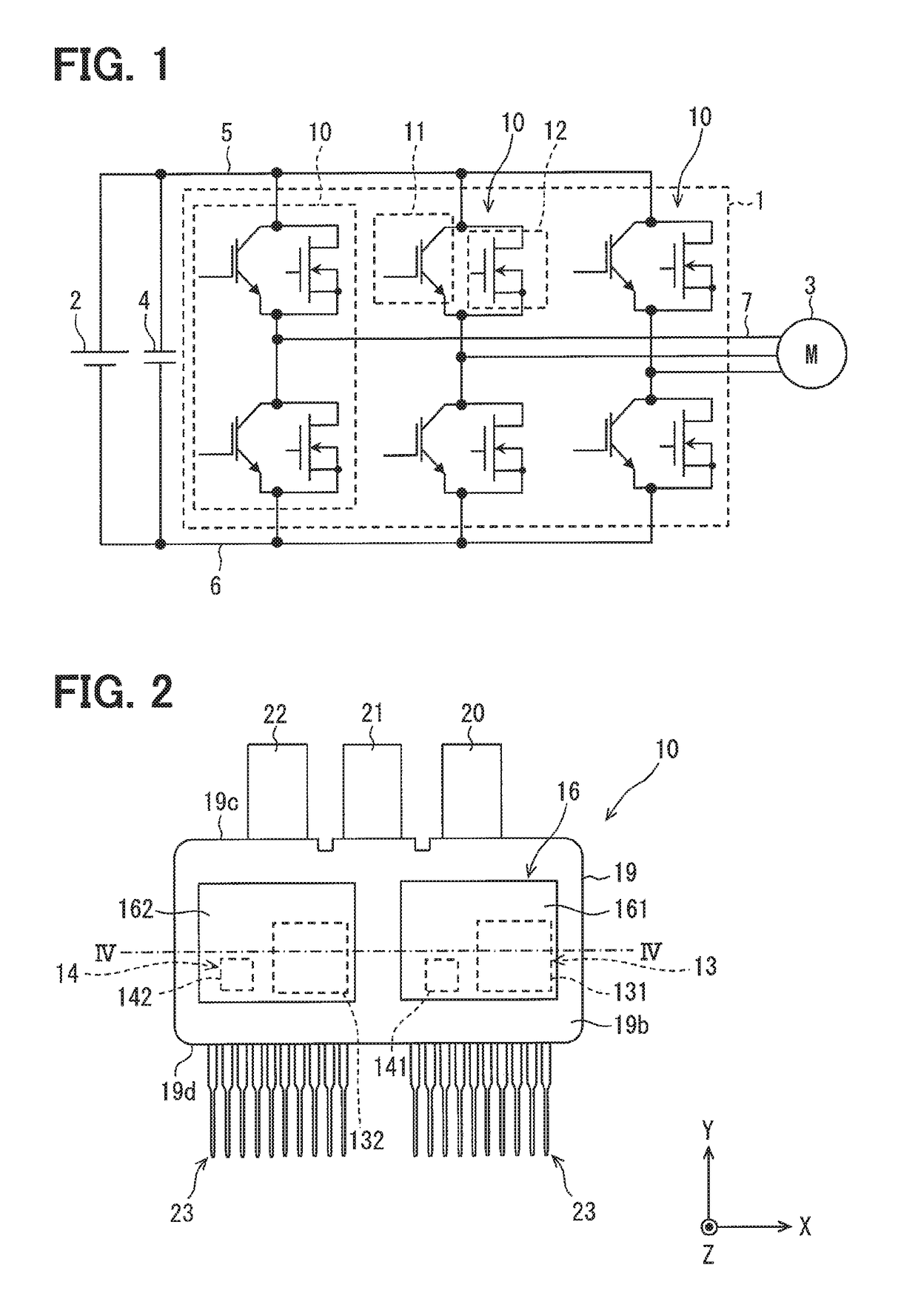
[0033]An example of an electrical power conversion device in which a semiconductor device is employed will be described with reference to FIG. 1.

[0034]An electrical power conversion device 1 shown in FIG. 1 converts a direct current (DC) voltage supplied from a DC power source 2 into a three-phase alternating current (AC), and outputs the three-phase AC to a motor 3 that is a three-phase AC motor. The electrical power conversion device 1 is mounted to, for example, an electrical vehicle or a hybrid vehicle. The electrical power conversion device 1 may convert an electrical power generated by the motor 3 into a DC power and may charge the DC power source 2 (e.g., a battery). Therefore, the motor 3 may be referred to as a motor generator. An element designated by a symbol 4 in FIG. 1 is a smooth capacitor 4.

[0035]The electrical power conversion device 1 has a three-phase inverter. The three-phase inverter includes three phases of upper and lower arms disposed between a high-potential ...

second embodiment

[0096]In a second embodiment, portions that are common to the semiconductor device 10 described in the first embodiment will not be repeatedly described.

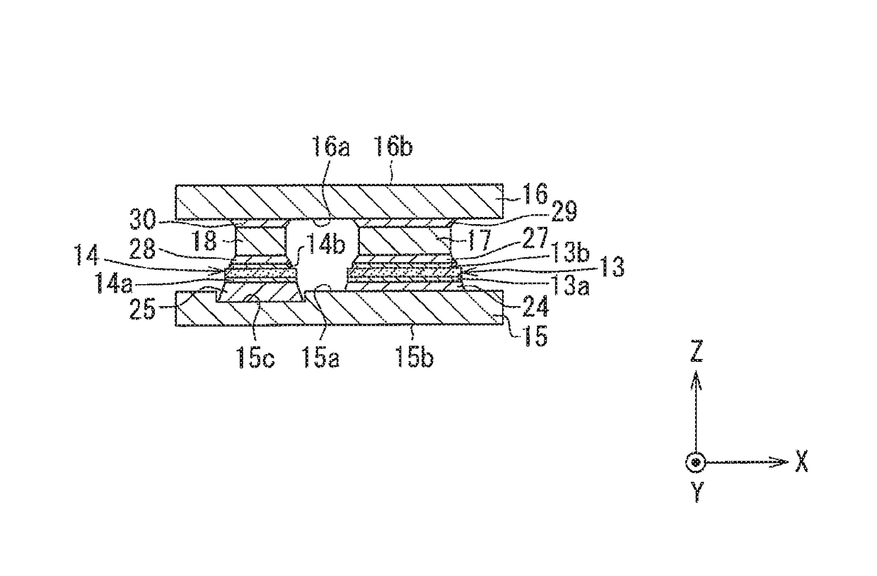
[0097]As shown in FIG. 7, in the second embodiment, the thickness of the solder 25 is greater than the maximum thickness of the first solder 24 at an entire periphery of the outer peripheral edge of the drain electrode 14a. Specifically, as shown in FIG. 8, the recess 15c is annularly formed to include the entire periphery of the outer peripheral edge of the drain electrode 14a, that is, the second semiconductor chip 14. In FIG. 8, an inner peripheral edge of the recess 15c is shown by a broken line. Similarly to FIG. 6, the illustration of the solder 25 is omitted in FIG. 8.

[0098]In the second embodiment, similar effects to the first embodiment are achieved. Especially in the second embodiment, the thickness of the solder 25 is increased at the entire periphery of the outer peripheral edge of the drain electrode 14a, to which the t...

third embodiment

[0100]In a third embodiment, portions that are common to the semiconductor device 10 described in the first embodiment will not be repeatedly described.

[0101]In the third embodiment, the thickness of the solder 25 is greater than the maximum thickness of the first solder 24 at corners (i.e., angles) of the drain electrode 14a having almost planar rectangular shape. The drain electrode 14a is formed in almost the entire surface of the second semiconductor chip 14 facing the heat sink 15. The corners of the drain electrode 14a are almost coincident with the corners of the second semiconductor chip 14. Therefore, the thickness of the solder 25 is greater than the maximum thickness of the first solder 24 at the corners 14c of the second semiconductor chip 14 having almost planar rectangular shape.

[0102]Specifically, as shown in FIG. 9, the recesses 15c are respectively formed to correspond to four corners 14c of the second semiconductor chip 14. Each of the recesses 15c is integrally fo...


PUM


Abstract

A semiconductor device includes a metal member, a first semiconductor chip, a second semiconductor chip, a first solder and a second solder. A quantity of heat generated in the first semiconductor chip is greater than the second semiconductor chip. The second semiconductor chip is formed of a material having larger Young's modulus than the first semiconductor chip. The first semiconductor chip has a first metal layer connected to the metal member through a first solder at a surface facing the metal member. The second semiconductor chip has a second metal layer connected to the metal member through a second solder at a surface facing the metal member. A thickness of the second solder is greater than a maximum thickness of the first solder at least at a portion of the second solder corresponding to a part of an outer peripheral edge of the second metal layer.

Description

CROSS REFERENCE TO RELATED APPLICATIONS[0001]This application is the U.S. national phase of International Patent Application No. PCT / JP2016 / 002043 filed on Apr. 15, 2016 and is based on Japanese Patent Application No. 2015-100822 filed on May 18, 2015, the disclosure of which is incorporated herein by reference.TECHNICAL FIELD[0002]The present disclosure relates to a semiconductor device in which a first semiconductor chip and a second semiconductor chip formed of materials having different Young's modulus are arranged at the same surface of a metal member and are connected to the metal member through solders.BACKGROUND ART[0003]For example, a patent literature 1 discloses a semiconductor device in which a first semiconductor chip and a second semiconductor chip formed of materials having different Young's modulus are arranged at the same surface of a metal member and are connected to the metal member through solders.[0004]In the semiconductor device, a conductive pattern (hereinaft...

Claims


Application Information

Patent Timeline
Patent Type & Authority Patents(United States)
IPC IPC(8): H01L29/49H01L21/56H01L21/48H01L23/31H01L23/00H01L23/495H02P27/06
CPCH01L23/562H01L21/4825H01L21/4842H01L21/4871H01L21/565H01L23/3114H01L23/4952H01L23/49513H01L23/49548H01L23/49562H01L23/49568H01L23/49575H01L24/33H01L24/83H01L2224/3303H01L2224/83815H01L2924/10253H01L2924/10272H01L2924/13055H01L2924/13091H01L2924/14252H01L2924/351H02P27/06H01L23/40H01L2924/181H01L2224/40H01L2224/371H01L2224/37599H01L23/3107H01L23/4334H01L23/49524H01L2224/83385H01L24/29H01L24/32H01L2224/04026H01L2224/06181H01L2224/26175H01L2224/291H01L2224/32245H01L2224/33181H01L2224/48247H01L2224/73215H01L2224/73265H01L2224/2612H01L2924/00012H01L2924/00014H01L2924/014H01L2924/00
Inventor ONODA, KENJIOOMAE, SYOICHIROU
Owner DENSO CORP
Why Eureka
Try Eureka