Display device and method for driving same

a technology of a display device and a driving method, which is applied in the direction of semiconductor devices, instruments, electrical devices, etc., can solve the problems of image sticking, display quality deterioration, and the threshold voltage of thin film transistors changing due to degradation, so as to shorten the monitor time

Pending Publication Date: 2022-06-02
SHARP KK
View PDF0 Cites 3 Cited by
  • Summary
  • Abstract
  • Description
  • Claims
  • Application Information

AI Technical Summary

Benefits of technology

[0023]According to some embodiments of the present disclosure, a control terminal of a drive transistor included in the pixel circuit in the i-th row is connected to the data signal line in the j-th column via the write control transistor, and a second conduction terminal of the drive transistor is connected to the data signal line in the (j+1)-th column via the monitor control transistor. Thus, when the characteristic of the drive transistor included in each pixel circuit is detected, two adjacent data signal lines can be used as a write line (signal line for supplying a potential for writing to the pixel circuit) and a read line (signal line serving as a path for the measurement current). As a result, the processing of applying the desired potential to the write line and the processing of applying the desired potential to the read line can be performed in parallel, and the monitor time is shortened compared to the configuration in the related art.

Problems solved by technology

However, the threshold voltage of the thin film transistor changes due to degradation.
As a result, variations in luminance occur, and the display quality deteriorates.
As a result, image sticking occurs.

Method used


Image

  • Display device and method for driving same
  • Display device and method for driving same
  • Display device and method for driving same

Examples


first embodiment

1. First Embodiment

1.1 Overall Configuration and Operation Outline

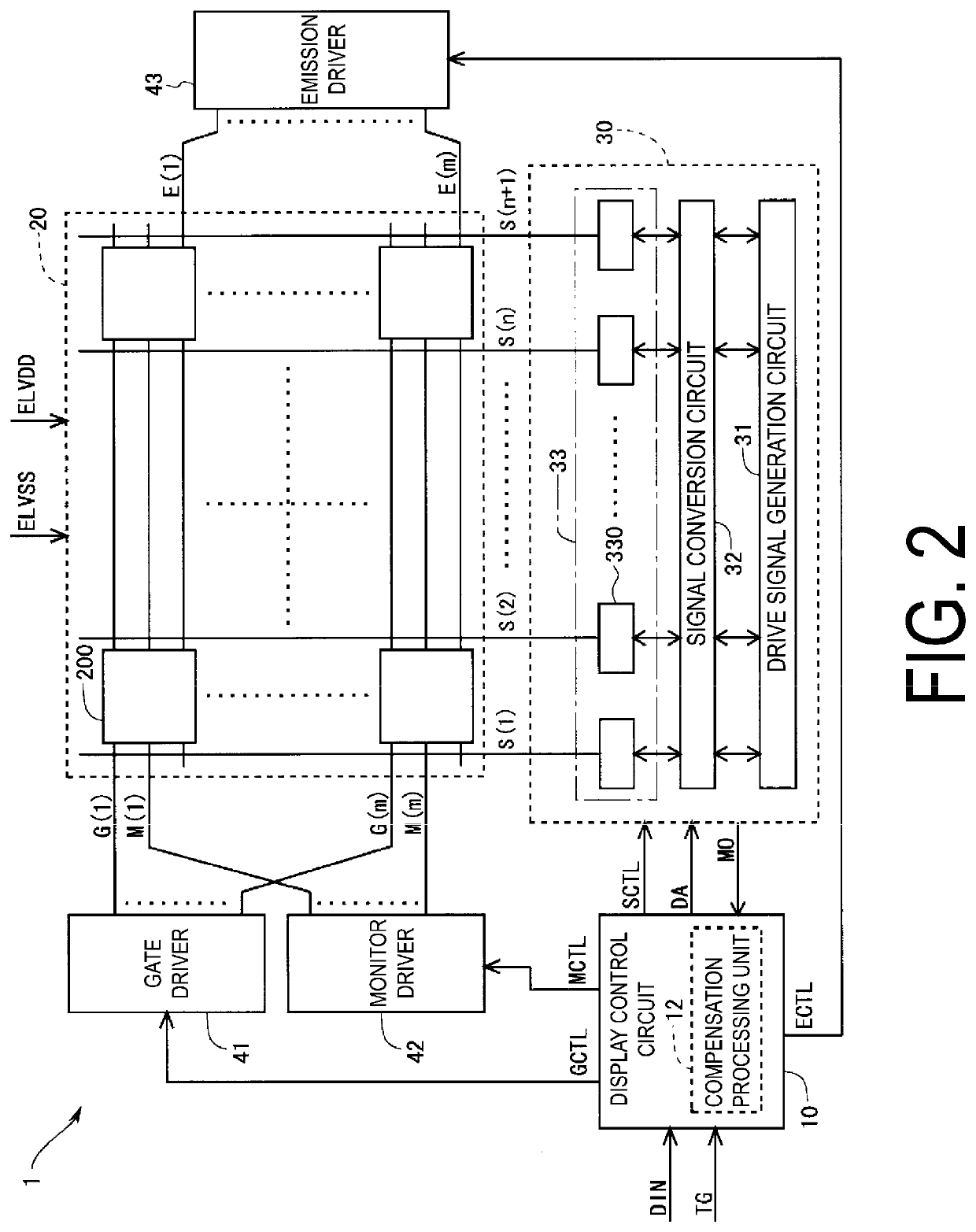
[0051]FIG. 2 is a block diagram illustrating an overall configuration of an active-matrix organic EL display device 1 according to the first embodiment. The organic EL display device 1 includes a display control circuit 10, a display portion 20, a source driver (data signal line drive circuit) 30, a gate driver (scanning signal line drive circuit) 41, a monitor driver (monitor control line drive circuit) 42, and an emission driver 43. Typically, the gate driver 41, monitor driver 42, and the emission driver 43 are formed to be monolithic. However, a configuration may also be used in which these drivers are not formed to be monolithic. The display control circuit 10 includes a compensation processing unit 12 that compensates for deterioration of drive transistors and organic EL elements.

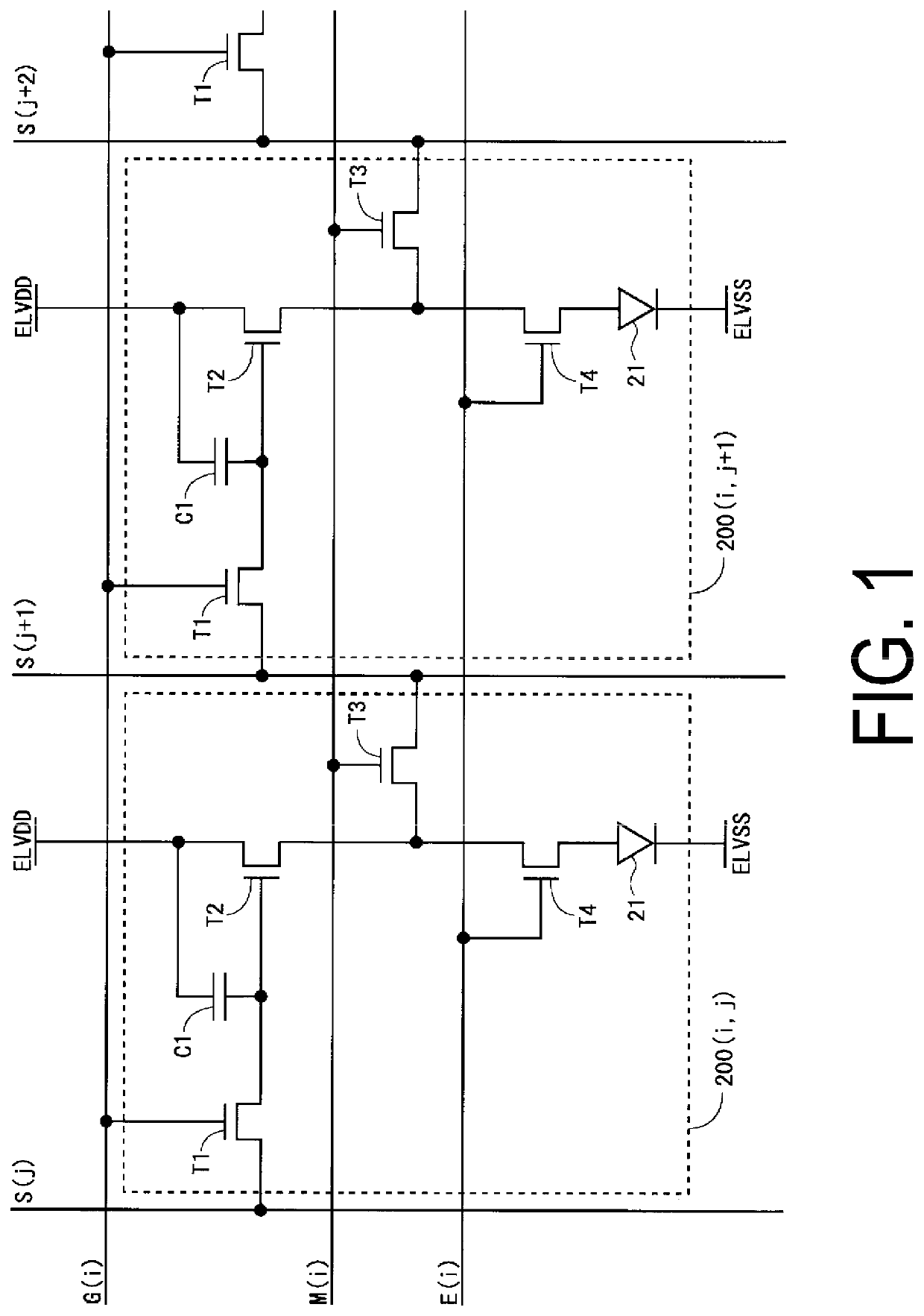
[0052]In the display portion 20, (n+1) data signal lines S(1) to S(n+1) and m scanning signal lines G(1) to G(m) orthogonal to the dat...

first modified example

1.6.1 First Modified Example

[0101]In the first embodiment described above, although when the TFT characteristic is detected, the application of the current measurement potential to the read line is started at the same timing as the application of the characteristic detection potential to the write line, when the OLED characteristic is detected, the application of the current measurement potential to the read line is started after a sufficient amount of time has elapsed from the application of the characteristic detection potential to the write line. However, the disclosure is not limited thereto, even when the OLED characteristic is detected, the application of the current measurement potential to the read line can be started at the same timing as the application of the characteristic detection potential to the write line.

[0102]FIG. 16 is a signal waveform diagram when the detection of the OLED characteristic is performed in the present modified example. The period t1 and previous p...

second modified example

1.6.2 Second Modified Example

[0105]In the first embodiment described above, with respect to the detection of the OLED characteristic, the characteristic detection for either the odd-numbered column or the even-numbered column is performed in each characteristic detection period. However, the disclosure is not limited thereto, and the detection of the OLED characteristic for all of the columns can also be performed in each characteristic detection period.

[0106]FIG. 18 is a signal waveform diagram when the detection of the OLED characteristic is performed in the present modified example. As can be seen from FIG. 18, the waveform of each signal for the j-th column and the (j+1)-th column change in the same manner. In other words, the waveform of each signal changes in the same manner in all columns. Operations related to the characteristic detection in the j-th column will be described below.

[0107]The period t1 and previous periods are similar to those in the first embodiment. In the p...


PUM


Abstract

With respect to a display device having an external compensation function, a monitor time can be shortened without increasing the number of wiring lines. A pixel circuit in an i-th row and a j-th column includes an organic EL element (display element), a writing control transistor, a drive transistor, a monitor control transistor, and a holding capacitor. A control terminal of the drive transistor is connected to a data signal line S(j) in the j-th column via the write control transistor. The monitor control transistor includes a first conduction terminal connected to a second conduction terminal of the drive transistor, and a second conduction terminal connected to a data signal line S(j+1) in a (j+1)-th column.

Description

TECHNICAL FIELD[0001]The following disclosure relates to a display device and a driving method thereof, and more specifically, relates to a display device including a pixel circuit including a display element (for example, an organic EL element) whose luminance is controlled by a current and to a driving method thereof.BACKGROUND ART[0002]Organic EL display devices including pixel circuits including organic EL elements have recently been coming into practical use. The organic EL element is also called an Organic Light-Emitting Diode (OLED) and is a self-luminous display element that emits light at luminance corresponding to a current flowing therethrough. As described above, since the organic EL element is a self-luminous display element, the organic EL display device can be easily thinned in size, reduced in power consumption, increased in luminance, and the like, as compared with a liquid crystal display device requiring backlights, color filters, and the like.[0003]In an active m...

Claims


Application Information

Patent Timeline
Patent Type & Authority Applications(United States)
IPC IPC(8): H01L27/32G09G3/3266G09G3/3275
CPCH01L27/3276H01L27/3265G09G2310/0278G09G3/3266G09G3/3275H01L27/3262G09G2320/0233G09G2320/043G09G2320/045G09G2320/029G09G2310/0262G09G2310/08G09G2300/0819G09G2300/0842G09G2300/0814H10K59/131H10K59/1213H10K59/1216
Inventor YAMAMOTO, KEIICHITANAKA, KOHHEINISHIYAMA, TAKAYUKI
Owner SHARP KK
Why Eureka
Try Eureka