Image display element
a technology of image and display element, applied in the direction of identification means, instruments, lenses, etc., can solve the problems of optical crosstalk, easy light leakage from one pixel to an adjacent pixel, etc., and achieve the effects of high color purity, low power consumption, and high contras
- Summary
- Abstract
- Description
- Claims
- Application Information
AI Technical Summary
Benefits of technology
Problems solved by technology
Method used
Image

Examples
embodiments
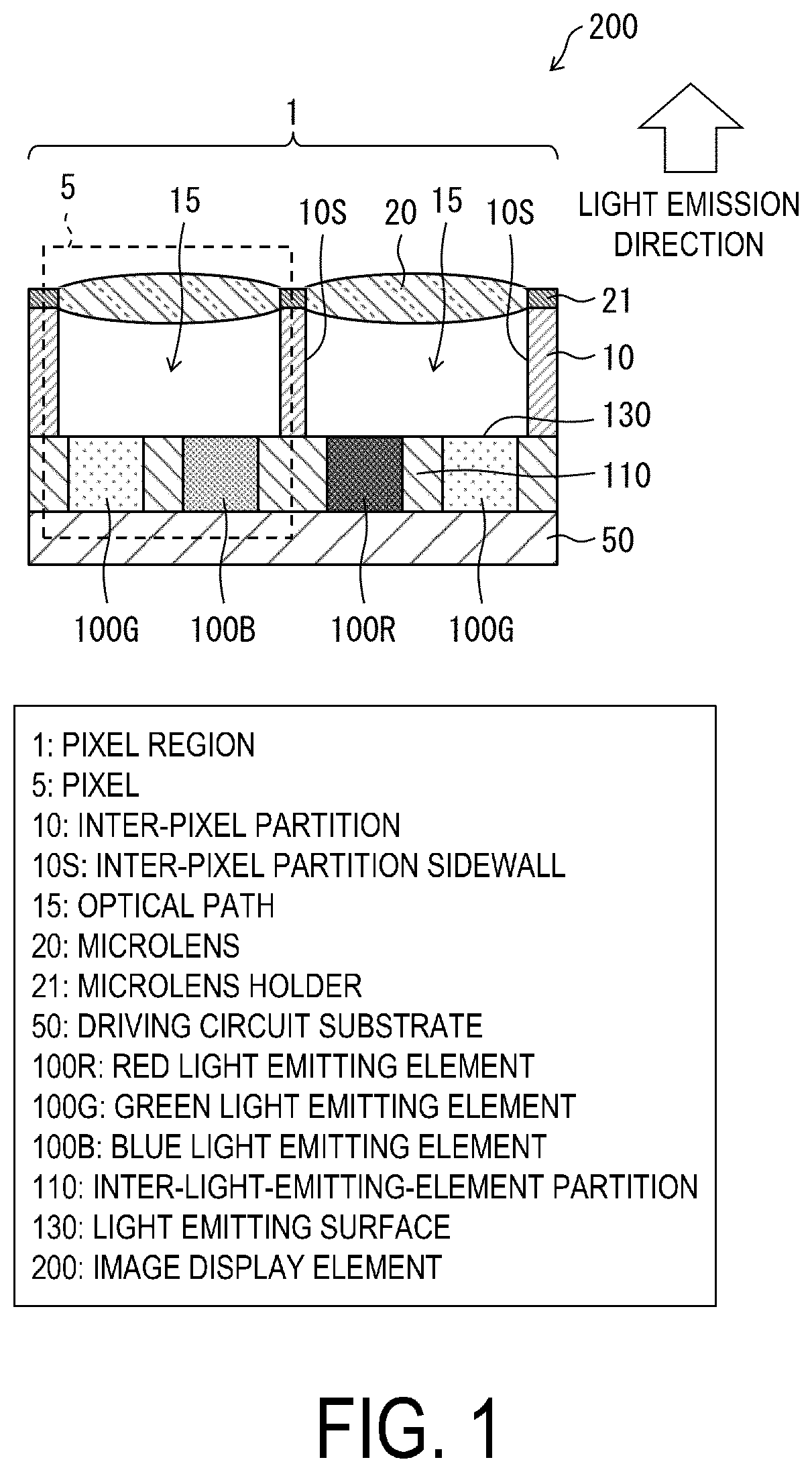
[0029]Embodiments according to an aspect of the present disclosure will be described below with reference to FIG. 1 to FIG. 10 using, as an example, an image display element including a plurality of micro light emitting elements. Note that the image display element includes the plurality of micro light emitting elements and a driving circuit substrate 50, and the driving circuit substrate 50 supplies a current to the micro light emitting elements disposed in a pixel region 1 and controls light emission.
[0030]The micro light emitting elements are disposed in an array in the pixel region 1. The micro light emitting elements emit light to a side opposite to the driving circuit substrate 50. The light emitted to the outside is referred to as emission light. Unless otherwise specified, a surface from which the light is emitted by the micro light emitting element is referred to as a light emitting surface.
[0031]Note that, when describing a configuration of the image display element, unles...
first embodiment
Configuration of Image Display Element 200
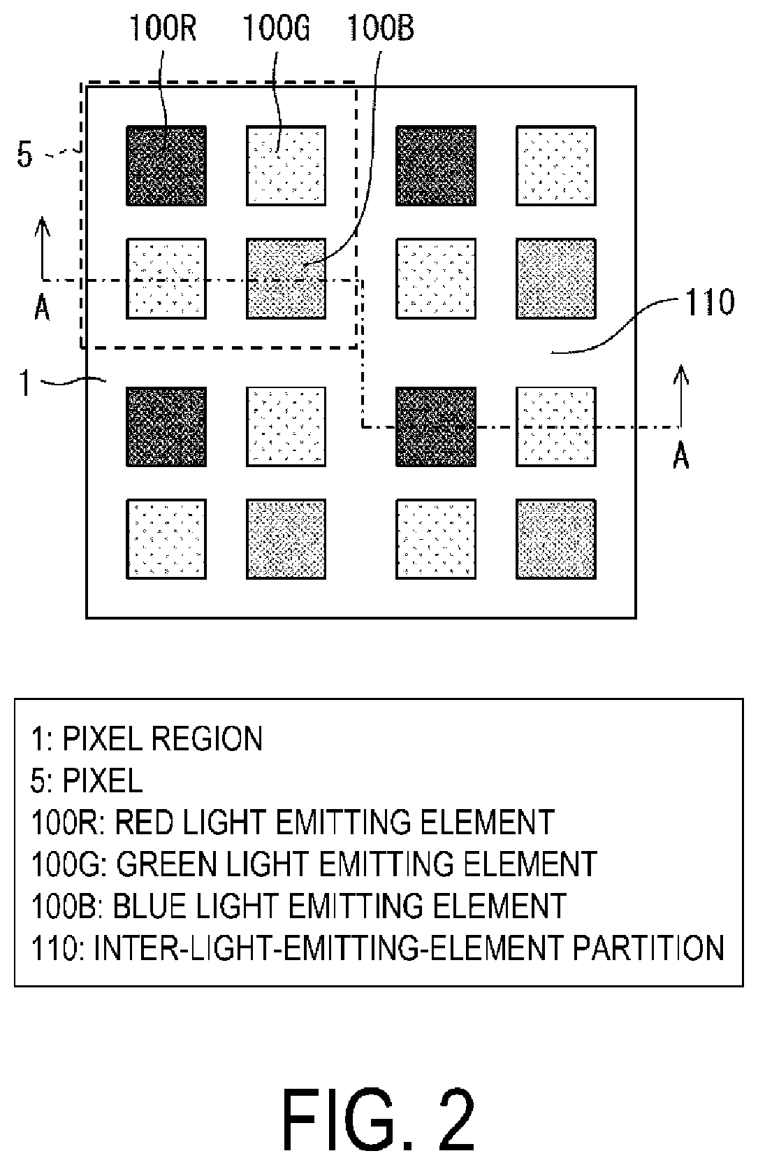
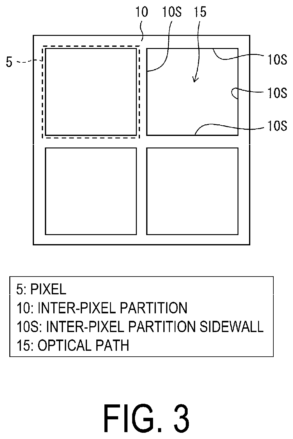
[0041]FIG. 1 is a schematic cross-sectional view of the pixel region 1 of the image display element 200 according to a first embodiment of the present disclosure. FIG. 2 is a schematic plan view of a light emitting surface 130 of the micro light emitting elements 100 according to the first embodiment of the present disclosure. As illustrated in FIG. 2, the upper surface of the image display element 200 is provided with the pixel region 1 which a plurality of pixels 5 are arranged in an array.
[0042]In the present embodiment, the image display element 200 is a full-color display element, and each of the pixels 5 includes one blue light emitting element 100B, two green light emitting elements 100G, and one red light emitting element 100R. Note that the blue light emitting element 100B, the green light emitting element 100G, and the red light emitting element 100R are collectively referred to as the micro light emitting elements 100. In this con...
second embodiment
[0060]A second embodiment will be described with reference to FIG. 5. In the first embodiment, both surfaces of the microlens 20 each have a convex shape; however, in an image display element 200a of the present embodiment, a microlens 20a has a convex shape on the micro light emitting element 100 side, but the surface on the light emission direction side is a plane. In other respects, there is no difference from the first embodiment.
[0061]In the image display element 200a, the thickness of a microlens holder 21a can be easily increased, and it is thus possible to increase the mechanical strength of the microlens array. As a result, the microlens array can be manufactured separately from the micro light emitting elements 100. For example, a glass substrate can serve as the microlens holder 21a, and the convex-shaped microlenses 20a can be formed on the glass substrate and then attached to the micro light emitting elements 100 via the inter-pixel partition 10. As a result, production...
PUM
 Abstract
Description
Claims
Application Information