Optical inspection apparatus in semiconductor process system

a technology of optical inspection and process system, applied in the direction of television system, test/measurement of semiconductor/solid-state devices, color television details, etc., can solve the problems of increasing stringent requirements of various detection apparatuses, manufacturing arrangement,

Pending Publication Date: 2022-06-30
CHROMA ATE
View PDF0 Cites 0 Cited by
  • Summary
  • Abstract
  • Description
  • Claims
  • Application Information

AI Technical Summary

Benefits of technology

[0005]It is an object of the present invention to provide an optical detection apparatus that can be readily mounted.
[0006]It is another object of the present invention to eliminate image deformation or a reduced resolution.
[0008]In one embodiment of the present invention, a center axis of a photosensitive surface of the photosensitive element may deviate from the optical axis of the lens group by a predetermined distance in a direction away from the movement path.
[0014]Accordingly, the optical detection apparatus disclosed is capable of avoiding other devices moving vertically above a wafer, and the special axial and horizontal motion design also prevents image deformation or a reduced resolution easily caused by capturing at an oblique angle, so that the optical detection apparatus resolves complications of additionally mounting an optical detection apparatus in an optical detection environment within a narrow space.

Problems solved by technology

With the continual improvement of semiconductor manufacturing processing capabilities, requirements for wafers have become more stringent, and this results in demands of various detection apparatuses on production lines.
However, when a new optical detection apparatus is needed on an existing production line, it may be unfeasible to add the new optical detection apparatus frequently due to a limited space or without modifying various tools on the existing production line, causing manufacturing arrangement complications.
Even if an additional optical detection apparatus is added, the imaging quality may be poor as a result of unsatisfactory imaging conditions because of the limited space, for example, image deformation or a low resolution, further leading to manufacturing arrangement complications.

Method used


Image

  • Optical inspection apparatus in semiconductor process system
  • Optical inspection apparatus in semiconductor process system

Examples


Embodiment Construction

[0017]The technical characteristics, contents, advantages and effects of the present invention will become apparent from the following detailed description taken with the accompanying drawing.

[0018]Terms, such as “a”, “an” and “one”, are descriptive of a unit, component, structure, device, module, system, region or zone to serve an illustrative purpose and define the scope of the present disclosure. Thus, unless otherwise specified, the terms must be interpreted to also mean “one or at least one”, and their singular forms may also be plural forms.

[0019]Terms, such as “include”, “comprise”, “have” and the like, used herein are not restricted to essential elements disclosed herein; instead, the terms also apply to any other essential elements not definitely specified but inherently required for a unit, component, structure, device, module, system, region or zone.

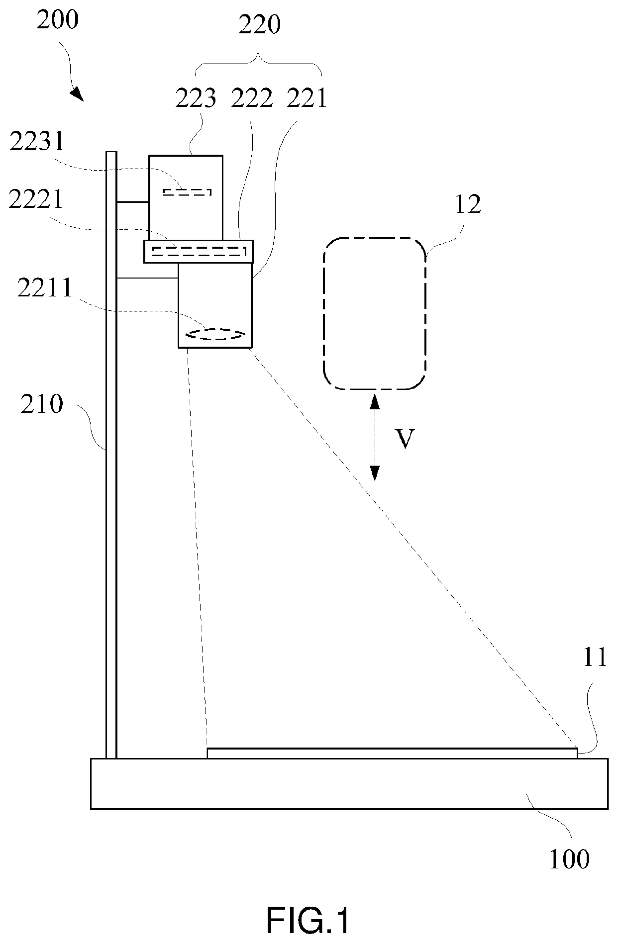
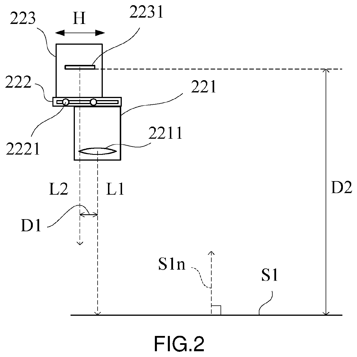
[0020]Referring to FIG. 1 and FIG. 2, FIG. 1 shows a schematic diagram of an optical detection apparatus according to an emb...


PUM

PropertyMeasurementUnit
vertical distanceaaaaaaaaaa
photosensitiveaaaaaaaaaa
lengthaaaaaaaaaa

Abstract

The present invention discloses an optical detection apparatus for defining a detection surface on a carrier unit for a wafer in a semiconductor manufacturing process so as to obtain a corresponding detection image, wherein a vertical movement path for another device to move is defined above the carrier unit. The optical detection apparatus includes a support, and an imaging device disposed on the support and configured to be non-interfering with the movement path. The imaging device includes a lens group, an image capturing portion and a moving base. With the moving base, the photosensitive element of the image capturing portion is allowed to move horizontally relative to the lens group, and the imaging position can be adjusted, preventing image deformation or a reduced resolution easily caused by capturing at an oblique angle. Thus, the optical detection apparatus resolves complications of additionally mounting an optical detection apparatus in an optical detection environment within a narrow space.

Description

BACKGROUND OF THE INVENTIONFIELD OF THE INVENTION[0001]The present invention relates to an optical detection apparatus, and more particularly to an optical detection apparatus for defining a detection surface so as to obtain a corresponding detection image on a carrier unit of a wafer in a semiconductor manufacturing process.[0002]DESCRIPTION OF THE PRIOR ART[0003]In a semiconductor manufacturing process, a wafer needs to undergo various detections so as to ensure its quality. With the continual improvement of semiconductor manufacturing processing capabilities, requirements for wafers have become more stringent, and this results in demands of various detection apparatuses on production lines.[0004]An optical detection apparatus is a common detection means. Detection apparatuses of different properties are provided to a surface of a wafer with numerous detection conditions so as to obtain detection images for read-end evaluation of the quality of the wafer. However, when a new optic...

Claims


Application Information

Patent Timeline
Patent Type & Authority Applications(United States)
IPC IPC(8): H01L21/66H04N5/232
CPCH01L22/12H04N5/23299H01L21/67288H04N23/00H04N23/695
Inventor PAN, SHIH-YAOKAO, HUNG-TIEN
Owner CHROMA ATE
Why Eureka
Try Eureka