Display device using semiconductor light emitting diode

a light-emitting diode and display device technology, applied in the field of display devices, can solve the problems of difficult flexibility implementation, short lifespan and production yield weakness of amoled, and achieve the effects of maximizing light collection efficiency, efficient light collection, and improving light collection efficiency

Pending Publication Date: 2022-07-07
LG ELECTRONICS INC
View PDF0 Cites 0 Cited by
  • Summary
  • Abstract
  • Description
  • Claims
  • Application Information

AI Technical Summary

Benefits of technology

[0020]A display device using a semiconductor light emitting diode according to an embodiment of the present disclosure has an effect of efficiently collecting light emitted from the semiconductor light emitting diode to a front surface of a panel due to the shape and structural characteristics of a hole in which the semiconductor light emitting diode is disposed.
[0021]Specifically, a reflective layer formed along the inner surface of the hole can reflect light leaking through the side or rear surface of the semiconductor light emitting diode toward the front surface of the panel, and the structure of the hole in which the width increases as a distance from a substrate increases and the vertical cross-section is symmetrical has an effect of improving the light collection efficiency.
[0022]In addition, the present disclosure has an effect of maximizing the light collection efficiency by applying the structure of the hole changed according to the shape, thickness, structure, and the like of the semiconductor light emitting diode disposed inside the hole.
[0023]Furthermore, since a first portion and / or a second portion extending from the reflective layer formed on the inner surface of the hole are included, the present disclosure has an effect of maintaining the light collection efficiency by supplementing the positional precision in a process of assembling the semiconductor light emitting diode.

Problems solved by technology

However, the LCD has disadvantages in terms of slow response time and difficult implementation of flexibility, and the AMOLED has weaknesses in terms of short lifespan and production yield.
However, a conventional display device using a micro-LED has a structure in which the micro-LED emitting light is surrounded by a transparent layer, and light loss occurs in the rear and side surfaces of a panel, which deteriorates image quality of the display device.

Method used


Image

  • Display device using semiconductor light emitting diode
  • Display device using semiconductor light emitting diode
  • Display device using semiconductor light emitting diode

Examples


Embodiment Construction

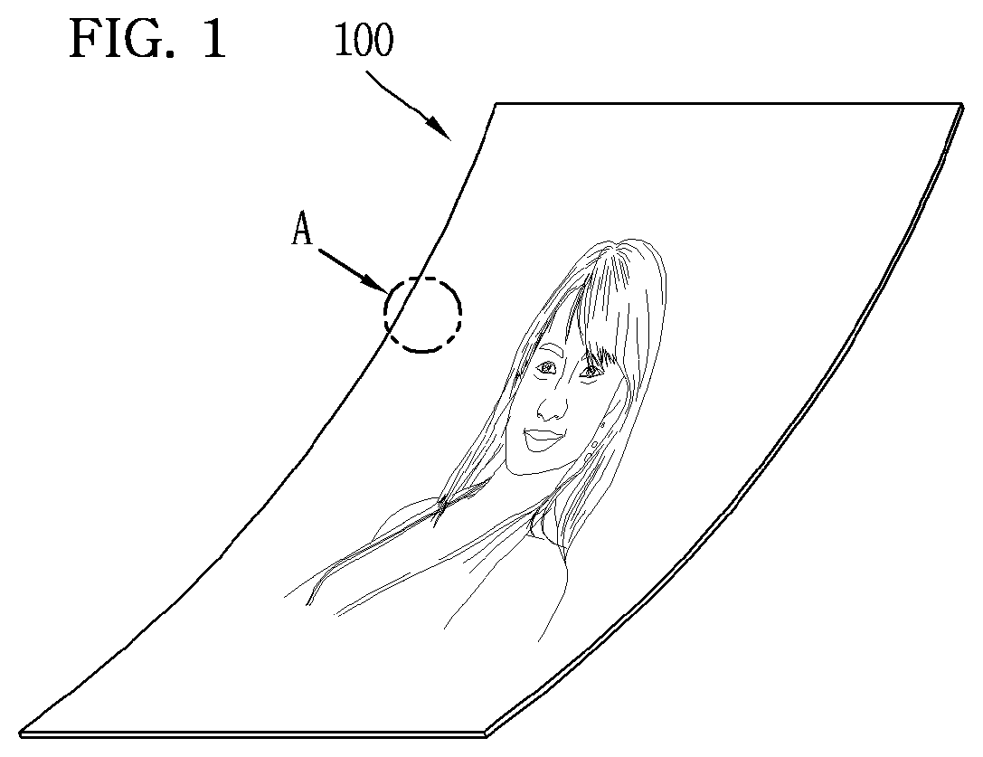
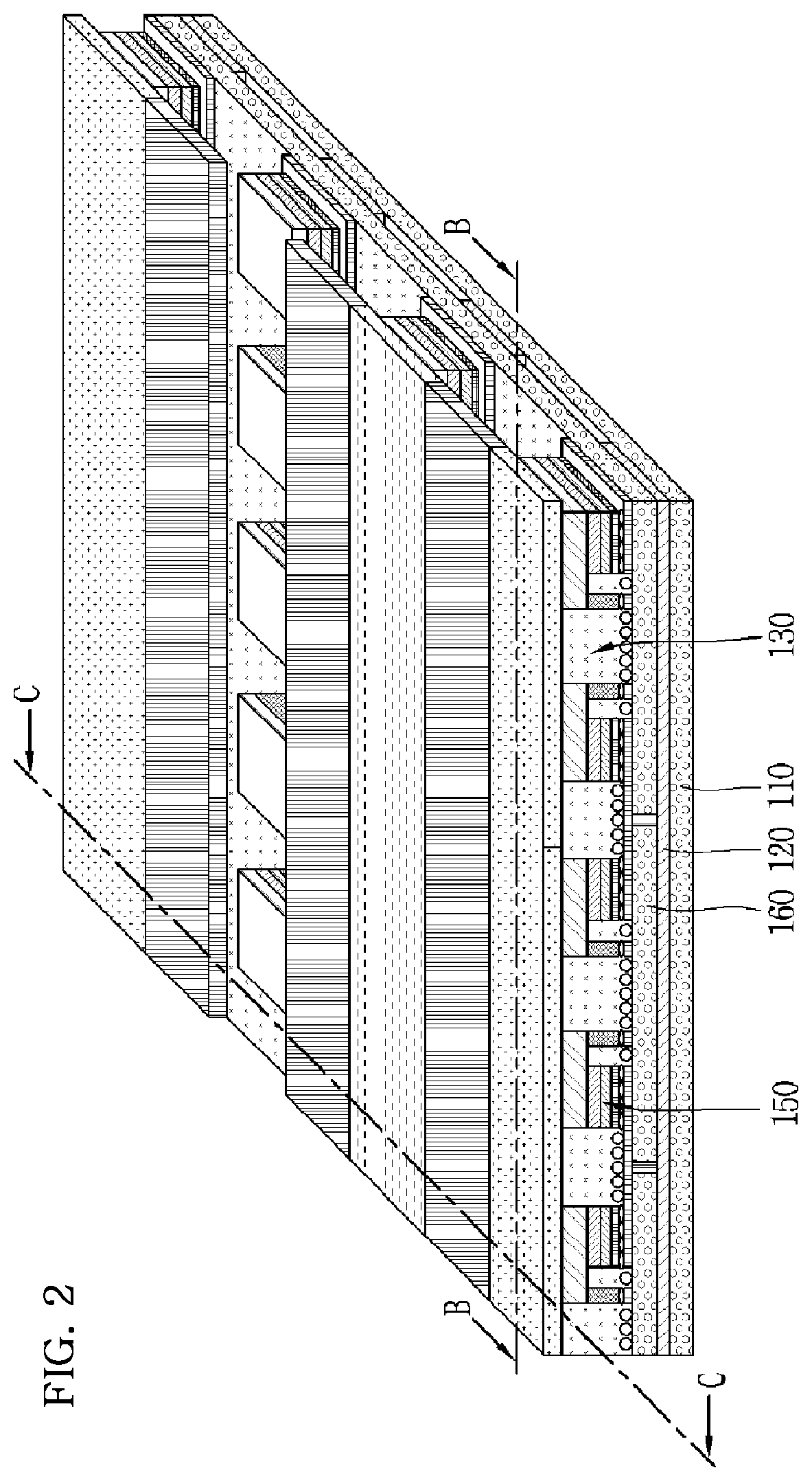
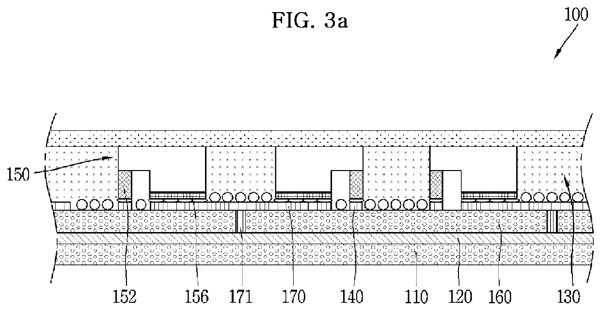
[0037]Hereinafter, embodiments of the present disclosure are described in detail with reference to accompanying drawings and regardless of the reference symbols, same or similar components are assigned with the same reference numerals and thus overlapping descriptions for those are omitted. The suffixes “module” and “unit” for components used in the description below are assigned or mixed in consideration of easiness in writing the specification and do not have distinctive meanings or roles by themselves. In the following description, detailed descriptions of well-known functions or constructions will be omitted since they would obscure the invention in unnecessary detail. Additionally, the accompanying drawings are used to help easily understanding embodiments disclosed herein but the technical idea of the present disclosure is not limited thereto. In addition, when an element such as a layer, a region, or a substrate is referred to as being “on” another element, it will be underst...


PUM

PropertyMeasurementUnit
thicknessaaaaaaaaaa
sizeaaaaaaaaaa
sizeaaaaaaaaaa

Abstract

Discussed is a display device using a semiconductor light emitting diode disposed on a substrate, a planarization layer stacked on the substrate while defining a hole that is a region in which the semiconductor light emitting diode is disposed, a light-transmitting layer filling the hole, and a reflective layer formed along at least one surface of the substrate and the planarization layer defining an inner surface of the hole, wherein the hole is formed so that a width thereof expands as a distance from the substrate increases.

Description

TECHNICAL FIELD[0001]The present disclosure relates to a display device, and more particularly, to a display device using a semiconductor light emitting diode having a size of several μm to several tens of μm.BACKGROUND ART[0002]Recently, in the field of display technology, display devices with excellent characteristics, such as thin film display devices and flexible display devices, are under development. On the other hand, representative currently commercialized major displays are liquid crystal display (LCD) and active matrix organic light emitting diode (AMOLED). However, the LCD has disadvantages in terms of slow response time and difficult implementation of flexibility, and the AMOLED has weaknesses in terms of short lifespan and production yield.[0003]On the other hand, light emitting diodes (LEDs) are semiconductor light emitting diodes widely known to convert electric current into light. Starting with the commercialization of red LEDs using a GaAsP compound semiconductor in...

Claims


Application Information

Patent Timeline
Patent Type & Authority Applications(United States)
IPC IPC(8): H01L33/60H01L25/075
CPCH01L33/60H01L33/56H01L25/0753H01L33/54H01L25/167H01L27/156H01L33/36H01L24/32H01L33/62H01L2224/32227H01L2933/0058
Inventor PARK, SANGDAEPARK, SUNGJINUM, JAEGWANGYUH, HWANKUK
Owner LG ELECTRONICS INC
Why Eureka
Try Eureka