Semiconductor module

a technology of semiconductor modules and semiconductor elements, applied in the field of semiconductor modules, can solve the problems of breaking the semiconductor element, and increasing the current density of the electrode, and achieve the effect of suppressing the surge voltag

Active Publication Date: 2022-07-21
MITSUBISHI ELECTRIC CORP
View PDF0 Cites 0 Cited by
  • Summary
  • Abstract
  • Description
  • Claims
  • Application Information

AI Technical Summary

Benefits of technology

[0005]An object of the present disclosure is to provide a semiconductor module which, by adopting an electrode structure having a low inductance, suppresses a surge voltage even during high-speed switching operation of a switching element and miniaturization thereof is ensured.

Problems solved by technology

The electrode structure of Japanese Patent Application Laid-Open No. 6-21323 has a structure in which the parallel plate electrode has a plurality of right-angled portions; therefore, the path length for the current becomes long and the inductance of the electrode is raised, potentially breaking the semiconductor element due to the surge voltage occurring during the high-speed switching operation of the semiconductor element.
Further, a thick conductive material cannot be used due to the difficulty in processing thereof because of those many right-angled portions, this increases the current density in the electrode, leading to a higher inductance.
When high-speed switching is required, the allowable current value is to be lowered, limiting the current capacity.
Although the effective way to reduce the inductance is to reduce the current density of the electrodes, this will lead to a wider electrode when the electrodes cannot be made thicker, having posed the problem of difficulty in the miniaturization of the semiconductor module.

Method used


Image

  • Semiconductor module
  • Semiconductor module
  • Semiconductor module

Examples


embodiment 1

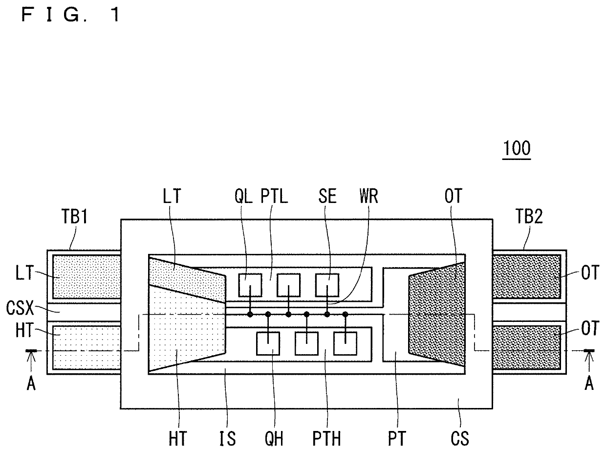
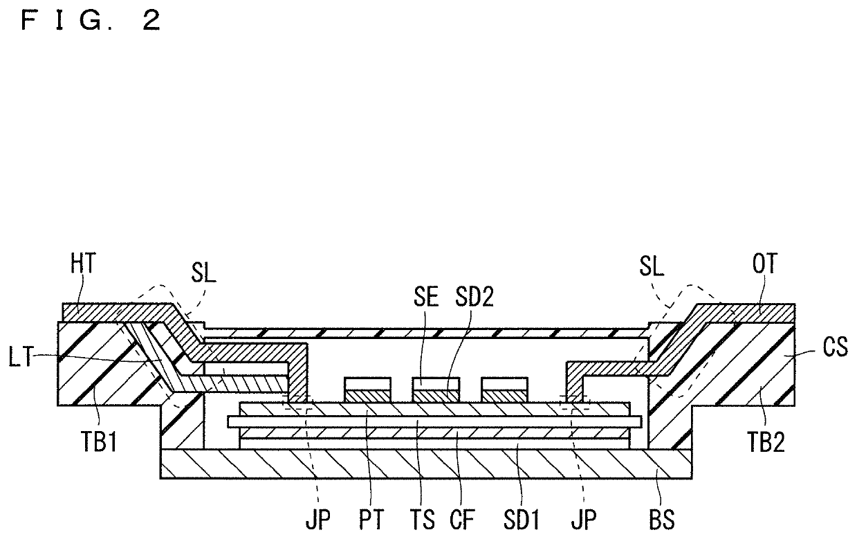
[0021]FIG. 1 is a plan view illustrating a configuration of a semiconductor module 100 according to Embodiment 1 and the upper surface of a resin case CS is omitted in order to clarify the internal configuration thereof. Further, FIG. 2 is a cross-sectional view illustrating the configuration of the semiconductor module 100, and is a cross-sectional view taken along the line A-A in FIG. 1 in the direction indicated by the arrows.

[0022]As illustrated in FIGS. 1 and 2, in the semiconductor module 100, the upper surface of a base plate BS that functions as a heat radiating plate and a conductor film CF on the lower surface of an insulating substrate IS are bonded via a bonding material SD1 such as a solder material. A circuit pattern PT is provided on the upper surface of the insulating substrate IS, and a plurality of semiconductor elements SE such as transistor chips for electric power and diode chips are bonded on the circuit pattern PT via a bonding material SD2 such as a solder ma...

embodiment 2

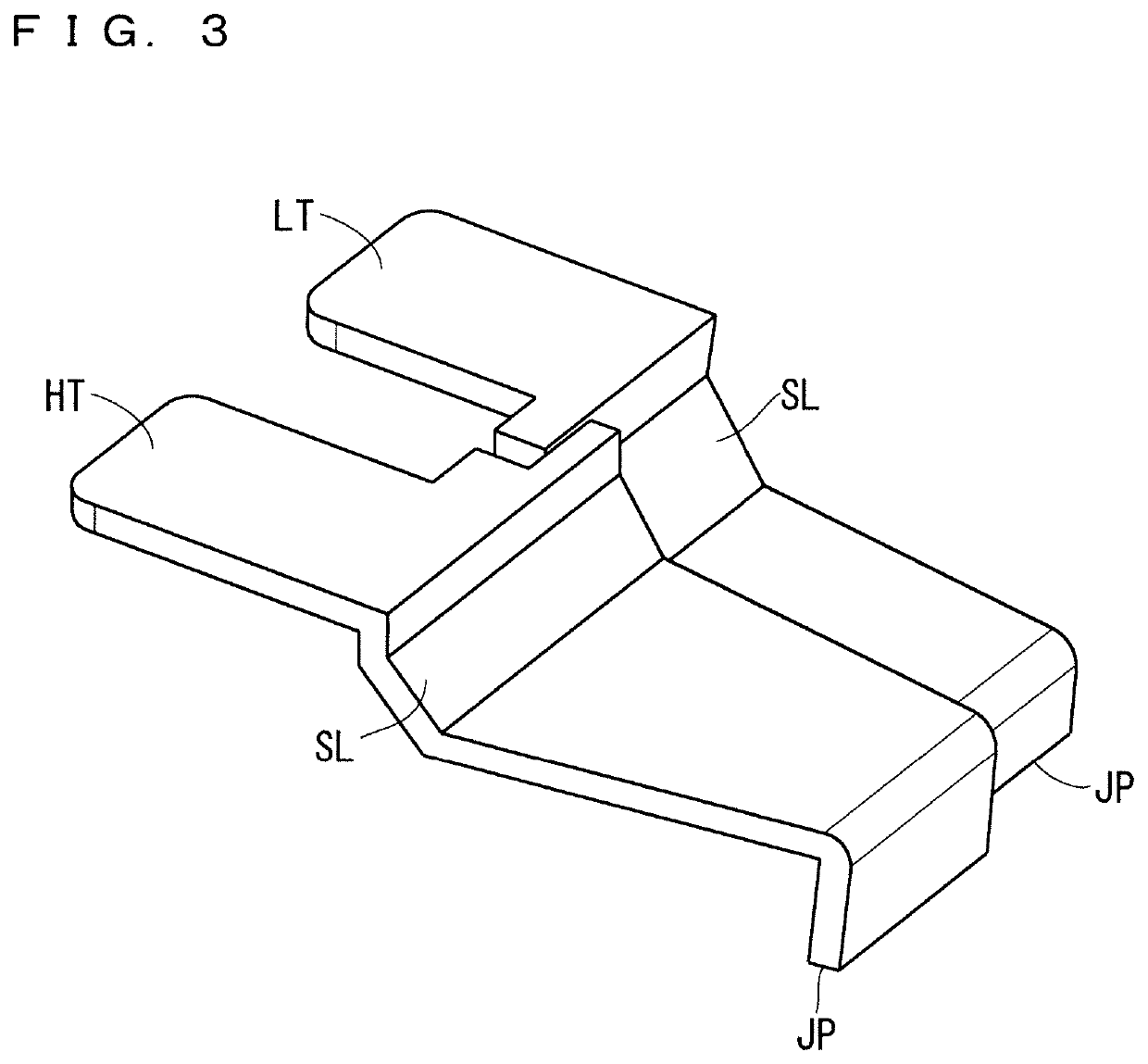
[0042]In the semiconductor module 100 of Embodiment 1 described above, although the configuration has been described in which the high potential electrode HT, the low potential electrode LT, and the output electrode OT all are provided with one slope portion SL, each electrode may be provided with a plurality of positions for the slope portions.

[0043]FIG. 9 is a cross-sectional view illustrating a configuration of a semiconductor module 200 of Embodiment 2, and is a view corresponding to the cross-sectional view in the direction indicated by the arrows along the line A-A in FIG. 1. In FIG. 9, the same components as those of the semiconductor module 100 described with reference to FIGS. 1 and 2 are designated by the same reference numerals, and duplicate description will be omitted.

[0044]As illustrated in FIG. 9, in the high potential electrode HT and the low potential electrode LT of the semiconductor module 200, one ends thereof are exposed on the upper surface of a terminal block ...

embodiment 3

[0048]FIGS. 10 and 11 are a plan view and a cross-sectional view illustrating a method of manufacturing a semiconductor module 300 of Embodiment 3, respectively. Noted that in FIGS. 10 and 11, the same components as those of the semiconductor module 100 described with reference to FIGS. 1 and 2 are designated by the same reference numerals, and duplicate description will be omitted.

[0049]As illustrated in FIGS. 10 and 11, the semiconductor module 300 includes a case CS in which the side wall of the case CS in which the high potential electrode HT and the low potential electrode LT are incorporated is formed as a separate body separated from an other part of the case CS and then a side wall CSX of the separate body is joined to the other part of the case CS by adhesive or the like to complete. Therefore, there is a seam between the side wall CSX and the other part.

[0050]Although the closer the distance between the electrodes of the high potential electrode HT and the low potential el...


PUM

PropertyMeasurementUnit
thicknessaaaaaaaaaa
angleaaaaaaaaaa
Comparative Tracking Indexaaaaaaaaaa

Abstract

A semiconductor module includes a semiconductor element, a substrate on which the semiconductor module is mounted, a heat radiating plate on which the substrate is mounted, a resin case, and a first main current electrode and a second main current electrode, in which in the first main current electrode and the second main current electrode, one end of each thereof is joined to a circuit pattern on the substrate, an other end of each thereof is extended through and incorporated in a side wall of the resin case so as to project outward of the resin case, and each thereof has at least a portion of overlap at which a part thereof overlaps in parallel with each other with a gap therebetween, and each thereof has a slope portion provided between an external projection portion and an internal projection portion.

Description

BACKGROUND OF THE INVENTIONField of the Invention[0001]The present disclosure relates to a semiconductor module, and more particularly to a semiconductor module having an electrode structure that reduces an inductance.Description of the Background Art[0002]Conventionally, as an electrode structure for suppressing a surge voltage on a power supply line of a semiconductor module, a structure disclosed in FIG. 1 of Japanese Patent Application Laid-Open No. 6-21323 has been proposed. In FIG. 1, two power supply terminals composed of plate-shaped conductors are provided close to each other with an insulating sheet having a thickness of 0.5 mm to 1.5 mm interposed therebetween. The currents flowing through the terminals are antiparallel to each other. It is disclosed that this lowers the inductance formed parasitically on the path formed by the two power supply terminals and the semiconductor element and lowers the surge voltage as well.[0003]The electrode structure of Japanese Patent App...

Claims


Application Information

Patent Timeline
Patent Type & Authority Applications(United States)
IPC IPC(8): H01L23/049H01L25/07H01L23/00H01L23/373
CPCH01L23/049H01L25/072H01L24/32H01L23/3735H01L2924/30107H01L2924/1715H01L2924/13055H01L2924/10272H01L2224/32225H01L23/62H01L23/053H01L23/04H01L21/50H01L2224/29101H01L24/29H01L23/49811H01L23/645H01L2924/014H01L2924/00014
Inventor GOTO, RYOSHIMIZU, YASUTAKA
Owner MITSUBISHI ELECTRIC CORP
Why Eureka
Try Eureka