

Switching element drive circuit
a technology of switching element and drive circuit, which is applied in the direction of pulse technique, power conversion system, oscillation generator, etc., can solve the problems of multiple series voltage converter, large variation in apportioning voltage, and possible breakage of switching element, and achieve short-circuit protection
- Summary
- Abstract
- Description
- Claims
- Application Information
AI Technical Summary
Benefits of technology
Problems solved by technology
Method used
Image

Examples
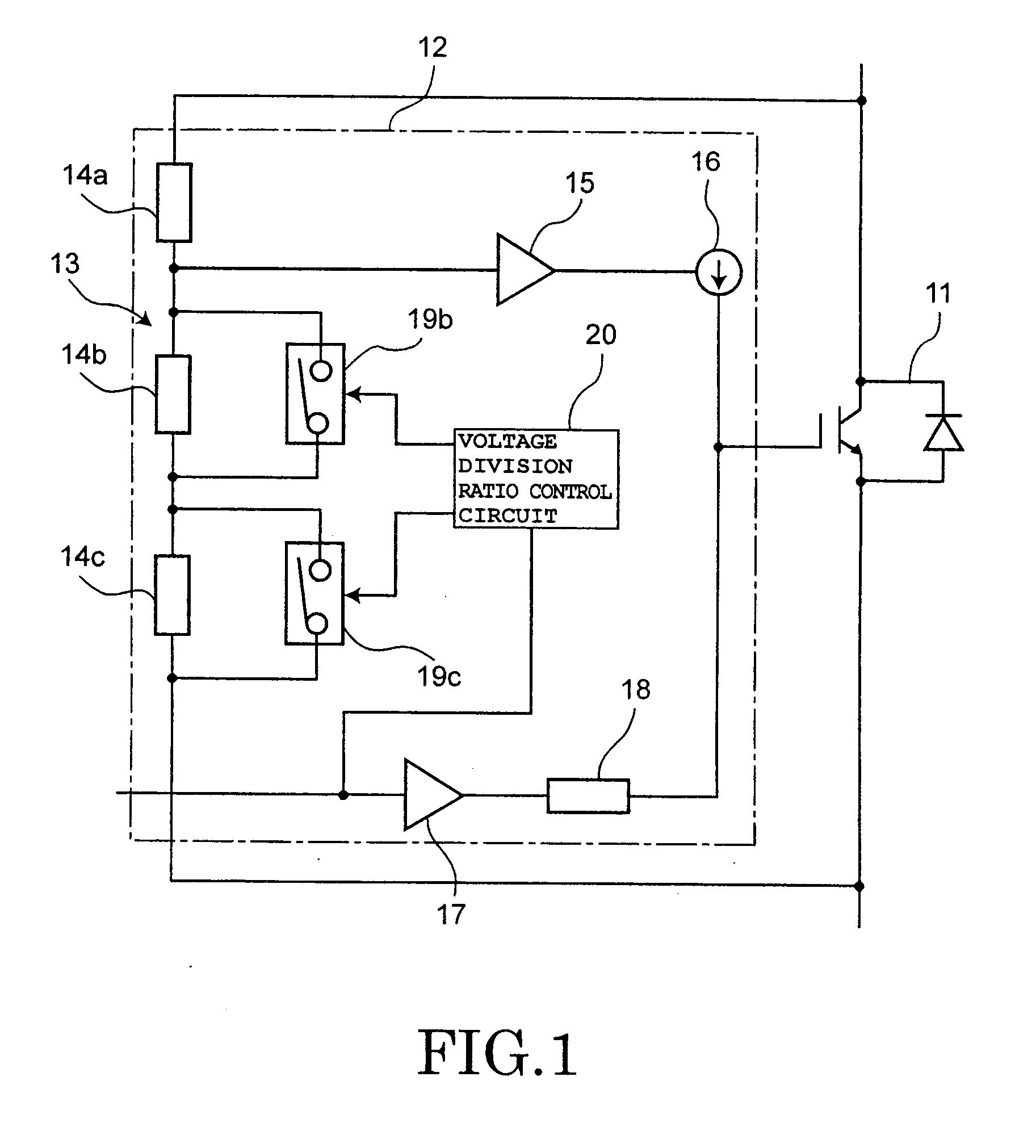
first embodiment
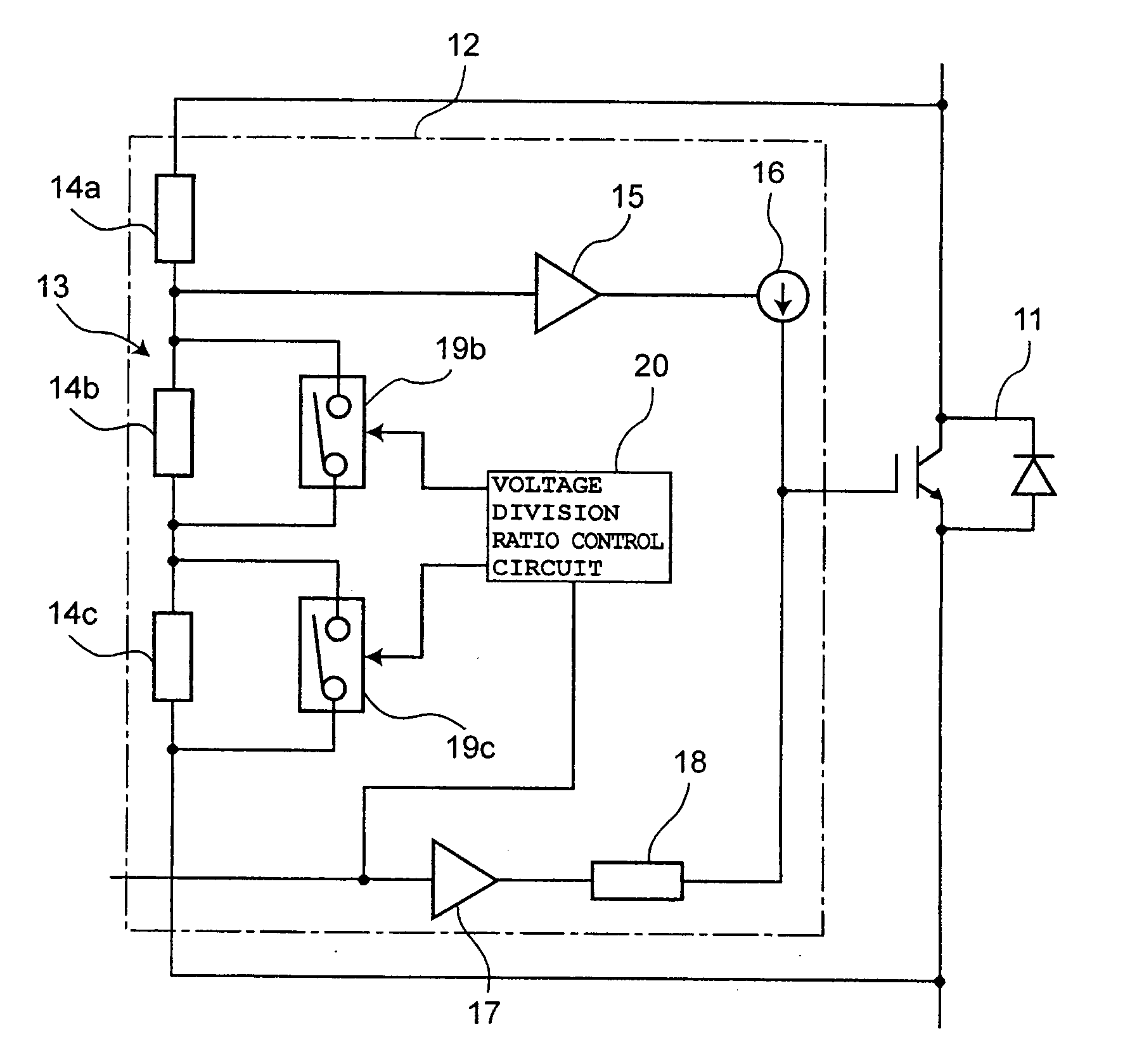
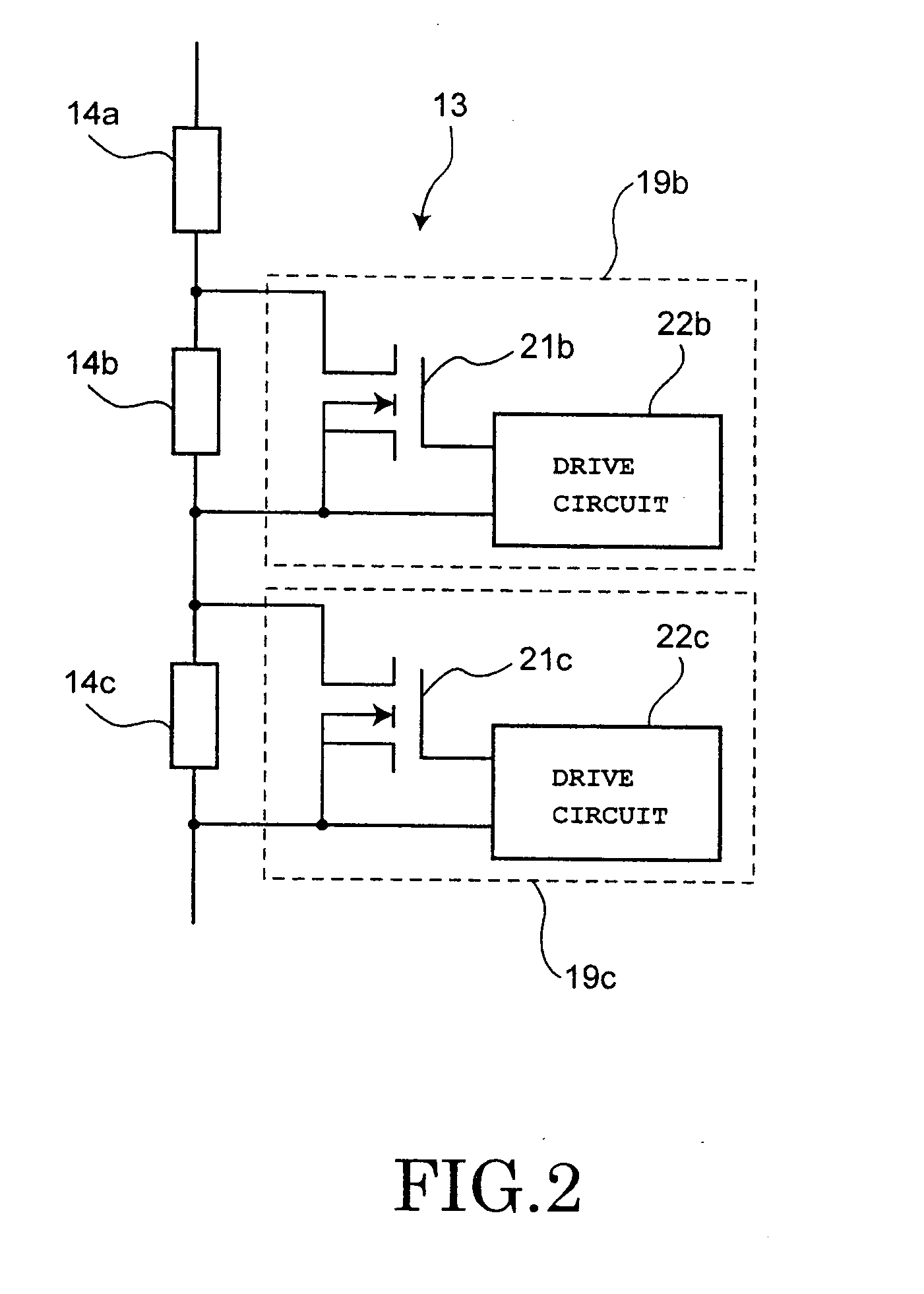
[0033]FIG. 1 is a layout diagram of a switching element drive circuit according to a first embodiment of the present invention. A gate electrode constituting a control electrode of the switching element 11 is provided with an active gate circuit 12 (indicated by the single-dotted chain lines). The active gate circuit 12 is connected between the two main electrodes of the switching element 11: the collector / emitter voltage of the switching element 11 is divided by voltage division elements 14a, 14b, 14c of a voltage division circuit 13, and the divided voltage of the main voltage detection voltage division elements 14b, 14c of the voltage division elements 14a, 14b, 14c of the voltage division circuit 13 is amplified by a voltage amplifier 15 and input to a control current source 16. Resistances or capacitors are employed as the voltage division elements 14a, 14b, 14c of the voltage division circuit 13.
[0034]The control current source 16 applies current to the control electrode of th...
second embodiment
[0042]FIG. 3 is a layout diagram of a switching element drive circuit according to a second embodiment of the present invention. In this second embodiment, compared with the first embodiment, a clamping circuit 23 is provided for clamping the gate voltage of the switching element 11 when the voltage of the main voltage detection voltage division elements 14b, 14c of the voltage division circuit 13 exceeds a prescribed value, and the voltage division ratio control circuit 20 is arranged to increase the voltage division ratio of the main voltage detection voltage division elements 14b, 14c of the voltage division circuit 13 immediately after turning-on of the switching element 11. Elements that are identical with corresponding elements in FIG. 1 are given the same reference symbols and repeated description is dispensed with.
[0043]When the switching element 11 is short-circuited, a current of several times the rated current flows in the switching element 11. A voltage determined by the...
third embodiment
[0046]FIG. 4 is a layout diagram of a switching element drive circuit according to a third embodiment of the present invention.
[0047]In this third embodiment, compared with the first embodiment, a turn-off detection circuit 24 is provided for detecting turn-off of the switching element 11 and the voltage division ratio control circuit 20 is arranged to increase the voltage division ratio of the main voltage detection voltage division elements 14b, 14c of the voltage division circuit 13 after turn-off of the switching element 11. Elements that are identical with corresponding elements in FIG. 1 are given the same reference symbols and repeated description is dispensed with.
[0048]In a circuit in which multiple switching elements 11 are connected in series, a specific switching element may be exposed to high voltage immediately after turn-off of the switching elements 11. This is determined by differences in the turn-off timing of the multiple series-connected switching elements 11 and...
PUM
 Abstract
Description
Claims
Application Information