Switching circuit

a switching circuit and circuit technology, applied in the field of switching circuits, can solve the problems of increasing the overall cost of the switching circuit, increasing the switching loss at the switching circuit, and prior art reducing the capacity of the capacitor, so as to reduce the switching loss and increase the current. , the effect of capacity variation

Inactive Publication Date: 2012-12-13
TOYOTA IND CORP
View PDF21 Cites 6 Cited by
  • Summary
  • Abstract
  • Description
  • Claims
  • Application Information

AI Technical Summary

Benefits of technology

[0013]According to this configuration, the plurality of insulated gate transistors are connected in parallel between the high voltage line and the low voltage line, and the first terminal of each gate resistor is connected to the gate electrode of each insulated gate transistor. Further, the second terminal of the gate resistor provided for each of the plurality of insulated gate transistors is connected to the gate voltage application unit via the gate voltage apply line, and the gate voltage application unit applies the pulsing gate voltage to the gate electrode of each insulated gate transistor via the corresponding gate resistor. As a result, the switching circuit can control a large current.
[0014]Further, the capacitor is connected to a single location between the gate voltage apply line and the high voltage line. By providing the capacitor, capacity variation between the gate electrodes of the insulated gate transistors and the high voltage line during gate voltage switching is suppressed. Hence, according to this configuration, switching loss can be reduced and a surge voltage can be suppressed with a compact configuration having a small amount of components.

Problems solved by technology

However, when the switching speed di / dt is reduced excessively with the aim of protecting the transistors from the surge voltage, another problem arises in that the switching loss at the switching circuit increases.
However, a switching circuit for controlling a large amount of power (large current) requires a snubber circuit having large capacity, and therefore the overall cost of the switching circuit increases.
Thus, for example, as the voltage between the drain electrode and the gate electrode increases, the prior art reduces the capacity of the capacitor.
In this case, an increase occurs in the number of components, leading to an increase in the overall size of the switching circuit.
For example, if only one transistor among four transistors 120, 121, 122 and 123 has a variable capacitor between the gate and drain electrode to reduce a number of components as shown in Japanese Laid-Open Patent Publication No. 2009-296216, there would be a problem in that current imbalance between transistors is caused upon driving the switching circuit to cause overheat and huge surge voltage in the switching circuit.

Method used


Image

  • Switching circuit
  • Switching circuit
  • Switching circuit

Examples


Embodiment Construction

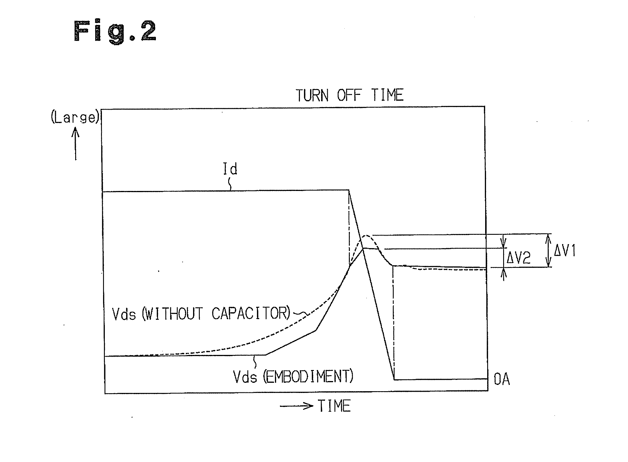
[0021]One embodiment of the present disclosure will be described below with reference to FIGS. 1 and 2.

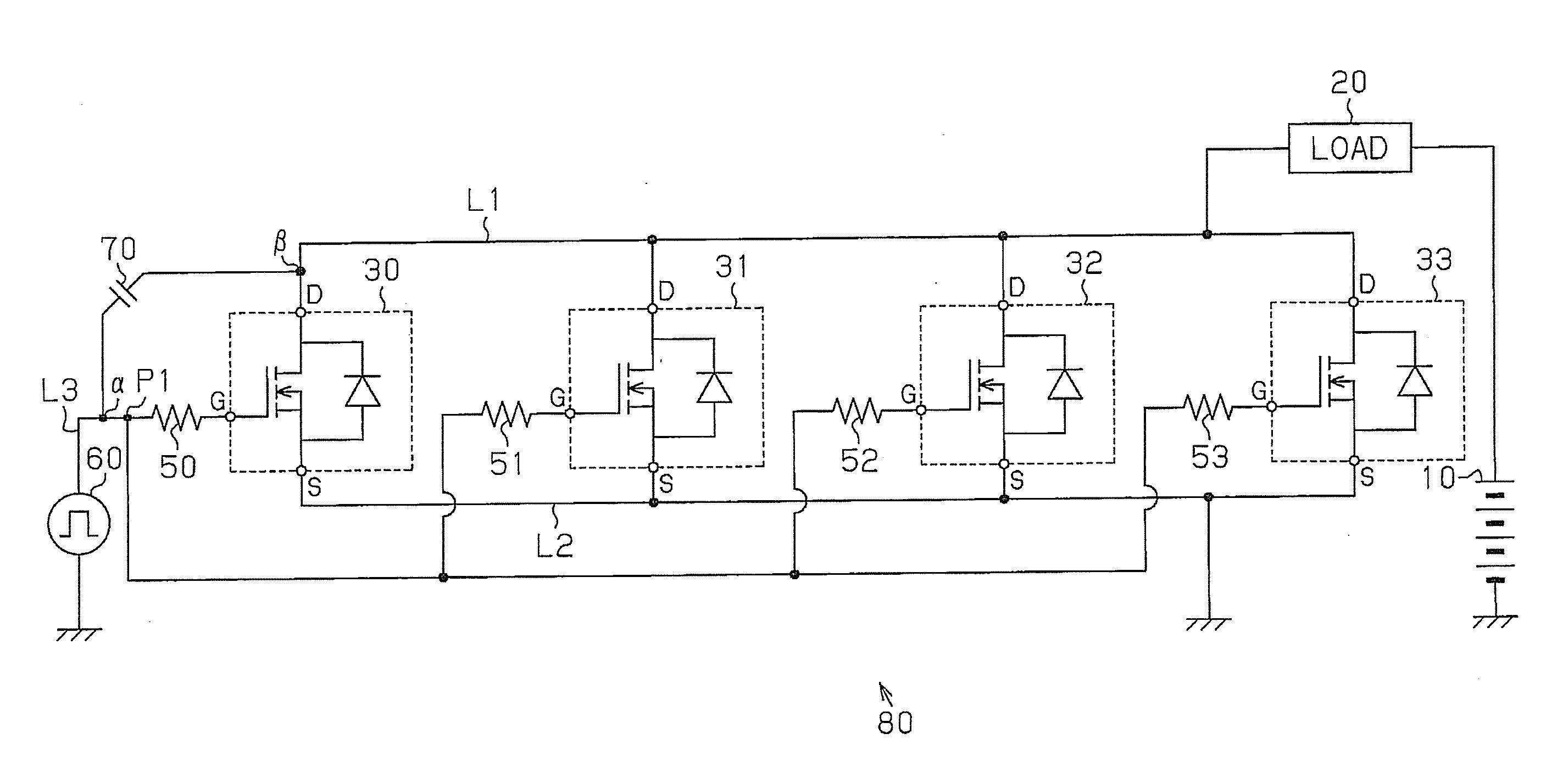
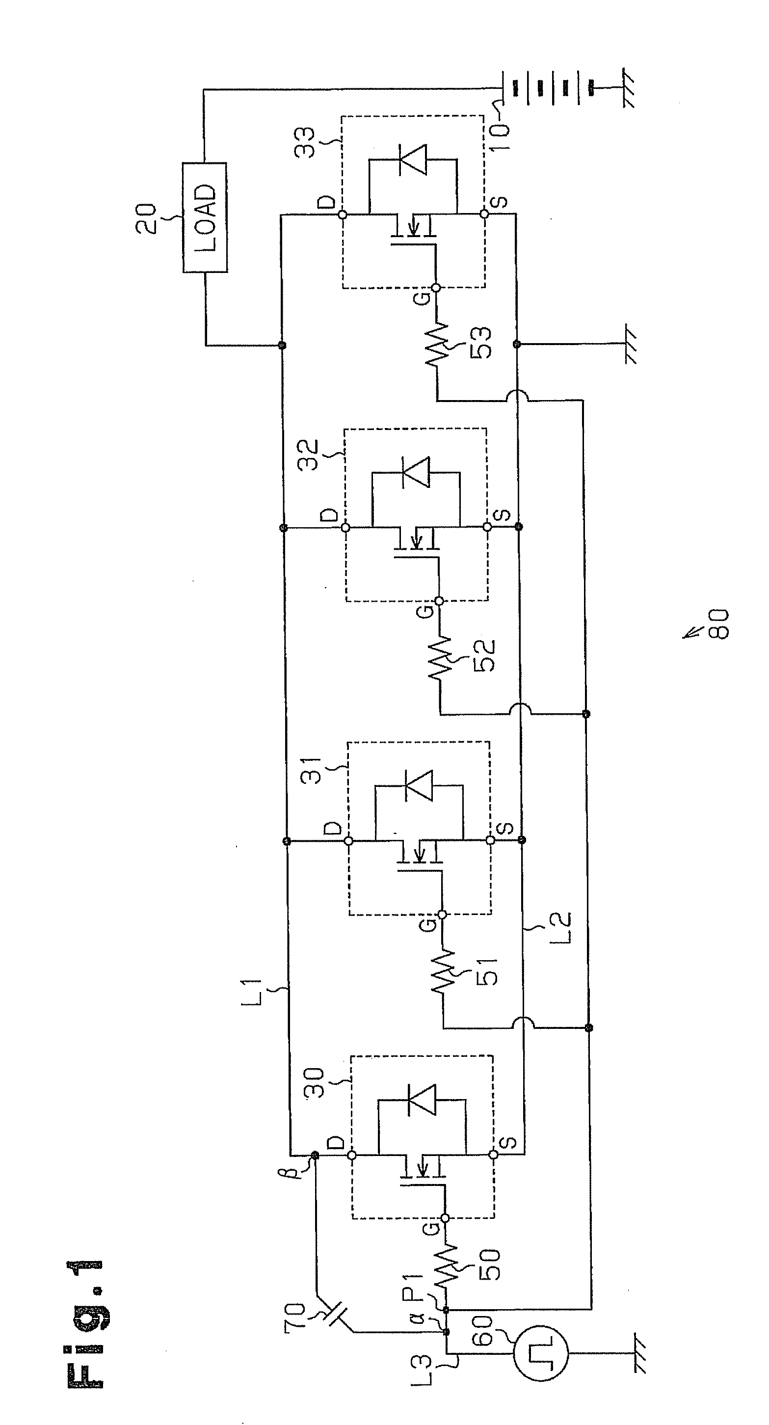
[0022]FIG. 1 is a circuit diagram of a switching circuit 80. The switching circuit 80 includes four MOSFETs 30, 31, 32, 33, gate resistors 50, 51, 52, 53 connected to gate electrodes of the respective MOSFETs 30, 31, 32, 33, a single pulse generator 60, and a single capacitor 70. The switching circuit 80 is connected to a load 20 which is connected to a direct current power supply 10.

[0023]As shown in FIG. 1, a negative electrode terminal of the direct current power supply 10 is grounded. The positive electrode terminal of the direct current power supply 10 is connected to one end of the load 20. The other end of the load 20 is connected to the drain terminals of the MOSFETs 30, 31, 32, 33, which serve as a plurality of insulated gate transistors connected in parallel, by a high voltage line L1. The source terminals of the MOSFETs 30, 31, 32, 33 connected in parallel are grounded b...


PUM


Abstract

A switching circuit (80) includes: a plurality of insulated gate transistors (30-33) connected in parallel between a high voltage line (L1) and a low voltage line (L2); gate resistors (50-53) each provided for one of the plurality of insulated gate transistors (30-33) and each including a first terminal connected to a gate electrode of each of the insulated gate transistors (30-33); and a single gate voltage application unit (60) configured to apply pulsing gate voltage to the gate electrode of each of the insulated gate transistors (30-33) via the gate resistors (50-53). A second terminal of each of the gate resistors (50-53) provided for each of the plurality of insulated gate transistors (30-33) is connected to the gate voltage application unit (60) via a gate voltage apply line (L3), and a single capacitor is connected between the gate voltage apply line (L3) and the high voltage line (L1).

Description

BACKGROUND OF THE INVENTION[0001]The present invention relates to a switching circuit.[0002]A switching circuit used in a DC-DC converter, an inverter, or the like has various requirements, such as small size and a small number of components, low ON resistance, low switching loss, and a low surge voltage.[0003]A switching circuit such as that described above uses MOSFETs, IGBTs, or the like. The switching circuit switches these transistors between an ON state and an OFF state by switching a gate voltage applied to the gate terminal, or in other words, a gate electrode, of each transistor. The speed of the switch, or in other words, the switching speed, is dependent on the parasitic capacity of the transistors, or in other words, the input capacity Ciss, the feedback capacity Crss, the output capacity Coss, as well as the resistance value of the gate resistor connected to the gate terminal. The input capacity Ciss is the sum of the gate-source capacity Cgs and the gate-drain capacity...

Claims


Application Information

Patent Timeline
Patent Type & Authority Applications(United States)
IPC IPC(8): H01L27/088
CPCH02M1/32H02M1/088H03K17/165H03K17/122H03K17/0822
Inventor KANIE, NAOHITONAGASE, TOSHIAKI
Owner TOYOTA IND CORP
Why Eureka
Try Eureka