Eureka AIR delivers breakthrough ideas for toughest innovation challenges, trusted by R&D personnel around the world.

Semiconductor package

Pending Publication Date: 2022-09-15
SAMSUNG ELECTRONICS CO LTD
View PDF0 Cites 0 Cited by
  • Summary
  • Abstract
  • Description
  • Claims
  • Application Information

AI Technical Summary

Benefits of technology

The patent describes a semiconductor package that is better for reliability and electric performance.

Problems solved by technology

In this case, since the under-bump patterns have a large pitch, an insulating layer between the under-bump patterns can shrink and cause an undulation phenomenon in the fine wire patterns.
The undulation phenomenon can decrease reliability of the semiconductor package.
However, this can deteriorate electric characteristics of the semiconductor package.

Method used


Image

  • Semiconductor package
  • Semiconductor package
  • Semiconductor package

Examples


Embodiment Construction

[0018]Embodiments of the inventive concepts will now be described more fully with reference to the accompanying drawings, in which embodiments are shown.

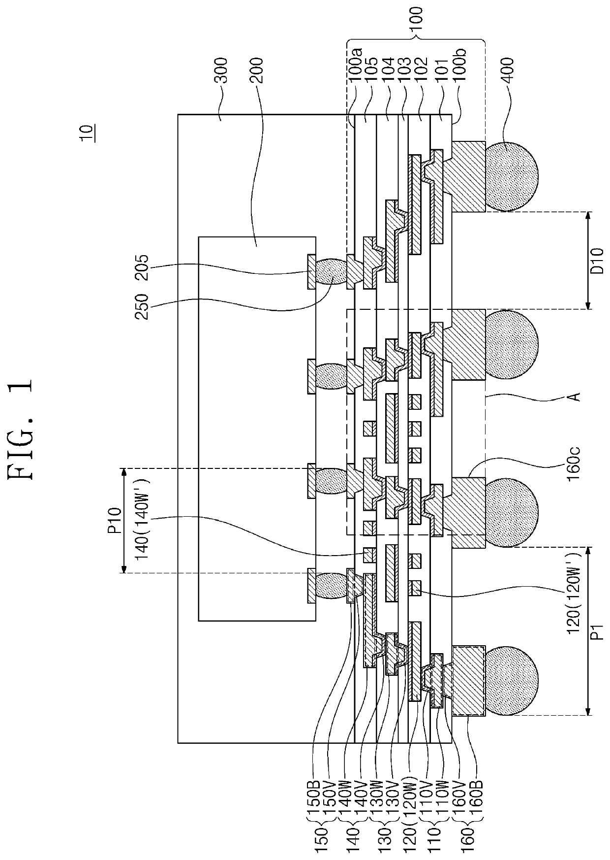
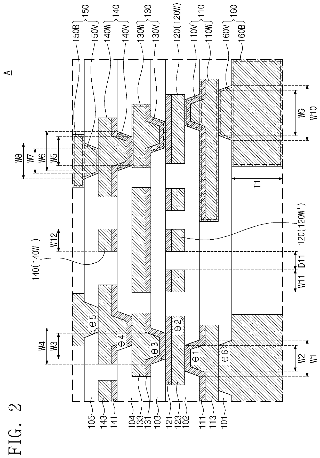
[0019]FIG. 1 is a sectional view of a semiconductor package according to an embodiment of the inventive concept. FIG. 2 is an enlarged sectional view of a portion ‘A’ of FIG. 1.

[0020]Referring to FIGS. 1 and 2, in some embodiments, a semiconductor package 10 includes a redistribution substrate 100 and a semiconductor chip 200. The redistribution substrate 100 includes insulating layers 101, 102, 103, 104, and 105, a first redistribution pattern 110, a second redistribution pattern 120, a third redistribution pattern 130, a fourth redistribution pattern 140, a bonding pad 150, and an under-bump pattern 160. The redistribution substrate 100 includes a top surface 100a and a bottom surface 100b, which are opposite to each other. The insulating layers include first to fifth insulating layers 101, 102, 103, 104, and 105, which are sequen...


PUM


Abstract

A semiconductor package includes a redistribution substrate and a semiconductor chip on a top surface of the redistribution substrate. The redistribution substrate includes an insulating layer, and first, second, and third redistribution patterns disposed in the insulating layer. The first to third redistribution patterns are sequentially stacked in an upward direction and are electrically connected to each other. Each of the first to third redistribution patterns includes a wire portion that extends parallel to the top surface of the redistribution substrate. Each of the first and third redistribution patterns further includes a via portion that extends from the wire portion in a direction perpendicular to the top surface of the redistribution substrate. The second redistribution pattern furthers include first fine wire patterns that are less wide than the wire portion of the second redistribution pattern.

Description

CROSS-REFERENCE TO RELATED APPLICATIONS[0001]This U.S. non-provisional patent application claims priority under 35 U.S.C. § 119 from Korean Patent Application No. 10-2021-0030913, filed on Mar. 9, 2021 in the Korean Intellectual Property Office, the contents of which are herein incorporated by reference in their entirety.BACKGROUNDTechnical Field[0002]Embodiments of the present disclosure are directed to a semiconductor package, and in particular, to a semiconductor package that includes a redistribution substrate.Discussion of the Related Art[0003]In a semiconductor package, a semiconductor chip is provided to be easily used as a part of an electronic product. Conventionally, a semiconductor package includes a printed circuit board (PCB) and a semiconductor chip, which is mounted on the PCB and is electrically connected to the PCB using bonding wires or bumps.[0004]In a conventional chip-last fan-out package, an under-bump pattern is formed when a redistribution substrate is formed...

Claims


Application Information

Patent Timeline
IPC IPC(8): H01L23/498H01L23/00H01L23/31
CPCH01L23/49816H01L23/49822H01L23/49838H01L24/04H01L23/3128H01L24/16H01L2224/0401H01L2224/16227H01L21/6835H01L2221/68345H01L21/56H01L2224/16225H01L2924/181H01L2924/15311H01L2224/73204H01L2224/32225H01L2224/81801H01L24/13H01L24/32H01L24/73H01L24/92H01L2224/92125H01L24/81H01L2924/15174H01L24/08H01L2224/08145H01L2924/18161H01L2924/15184H01L21/4857H01L2224/81484H01L2224/13116H01L2224/81447H01L2224/05599H01L2224/8349H01L2224/13113H01L2224/13139H01L2224/81424H01L2224/80379H01L2224/81466H01L2224/13111H01L2224/2919H01L2924/00012H01L2224/16145H01L2224/32145H01L2924/013H01L2924/00013H01L2924/0665H01L2924/00014H01L2924/06H01L2924/014H01L23/5389
Inventor JANG, JAEGWONSUK, KYOUNG LIMBAE, MINJUN
Owner SAMSUNG ELECTRONICS CO LTD
Why Eureka
Eureka Blog
Learn More