Semiconductor memory structure
a memory structure and semiconductor technology, applied in the direction of semiconductor devices, electrical equipment, transistors, etc., can solve the problems of many challenges
- Summary
- Abstract
- Description
- Claims
- Application Information
AI Technical Summary
Benefits of technology
Problems solved by technology
Method used
Image


Examples
Embodiment Construction
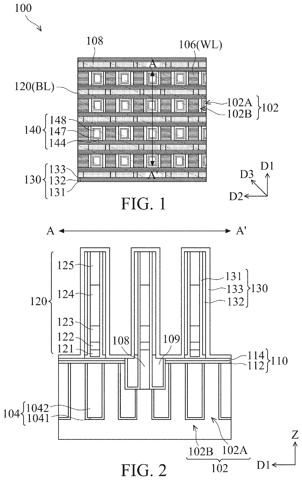
[0008]FIG. 1 illustrates a top view of a semiconductor memory structure 100 according to some embodiments of the present disclosure. In some embodiments, the semiconductor memory structure 100 is a portion of dynamic random access memory array. The semiconductor memory structure 100 includes a semiconductor substrate 102, a word line 106, a bit line contact 108, a bit line 120, a dielectric liner 130, and a capacitor contact 140.
[0009]The semiconductor substrate 102 includes an active region 102A and an isolation region 102B surrounding the active region 102A. The dielectric liner 130 includes a pair of nitride liners 131 and 133 and an oxide liner 132 sandwiched between the nitride liners 131 and 133. The capacitor contact includes a metal plug 144 and an adhesive layer 147 and a nitride layer 148 both surrounding the metal plug 144. It should be noted that only some of the elements of a DRAM are illustrated in FIG. 1 for brevity.
[0010]The word line 106 extends in a first direction...
PUM
 Abstract
Description
Claims
Application Information
 - R&D
- Intellectual Property
- Life Sciences
- Materials
- Tech Scout
- Unparalleled Data Quality
- Higher Quality Content
- 60% Fewer Hallucinations
Browse by: Latest US Patents, China's latest patents, Technical Efficacy Thesaurus, Application Domain, Technology Topic, Popular Technical Reports.
© 2025 PatSnap. All rights reserved.Legal|Privacy policy|Modern Slavery Act Transparency Statement|Sitemap|About US| Contact US: help@patsnap.com