Photoelectric conversion panel

a technology of photoelectric conversion panel and photoelectric converter, which is applied in the direction of electrical equipment, semiconductor devices, radio control devices, etc., can solve the problems of data line partially leakage through the protection diode into the electrostatic discharge protection constant potential line, and the scan line signals running in the scan line and the data line partially leak through the protection diode. to achieve the effect of reducing the influence of a resul

Pending Publication Date: 2022-11-17
SHARP DISPLAY TECH CORP
View PDF0 Cites 0 Cited by
  • Summary
  • Abstract
  • Description
  • Claims
  • Application Information

AI Technical Summary

Benefits of technology

[0005]Even if electro-static discharge enters the scan line and the data line during production of the photoelectric conversion panel according to Japanese Unexamined Patent Application Publication No. 2009-302092, the protection diode dissipates a current caused by the electro-static discharge in the electro-static-discharge-protection constant potential line, and prevents breakdown of an element in the pixel. However, when the photoelectric conversion panel according to Japanese Unexamined Patent Application Publication No. 2009-302092 is used in the solid-state imaging device for obtaining an image, a signal running in the scan line and the data line partially leaks through the protection diode into the electro-static-discharge-protection constant potential line. Such a leak might affect a result of the imaging.
[0006]The present disclosure is conceived in view of the above problem, and intended to provide a photoelectric conversion panel capable of preventing breakdown of an element in a pixel by electro-static discharge during production of the photoelectric conversion panel, and of reducing influence on a result of image obtainment while the image is obtained.
[0008]In the above photoelectric conversion panel, a depletion thin-film transistor for protection and an electro-static-discharge protection circuit can prevent an element in a pixel from breaking down by electro-static discharge during the production of the photoelectric conversion panel. In obtaining an image, an interrupting voltage is applied to the depletion thin-film transistor for protection. Hence, the depletion thin-film transistor for protection can block a signal from a gate line or a data line not to enter the electro-static-discharge protection circuit, thereby contributing to a reduction in influence on a result of obtaining the image.

Problems solved by technology

However, when the photoelectric conversion panel according to Japanese Unexamined Patent Application Publication No. 2009-302092 is used in the solid-state imaging device for obtaining an image, a signal running in the scan line and the data line partially leaks through the protection diode into the electro-static-discharge-protection constant potential line.
Such a leak might affect a result of the imaging.

Method used


Image

  • Photoelectric conversion panel
  • Photoelectric conversion panel
  • Photoelectric conversion panel

Examples


Embodiment Construction

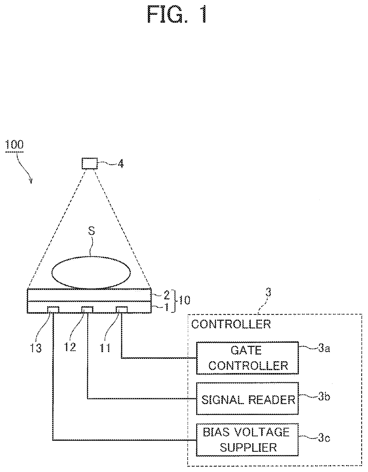
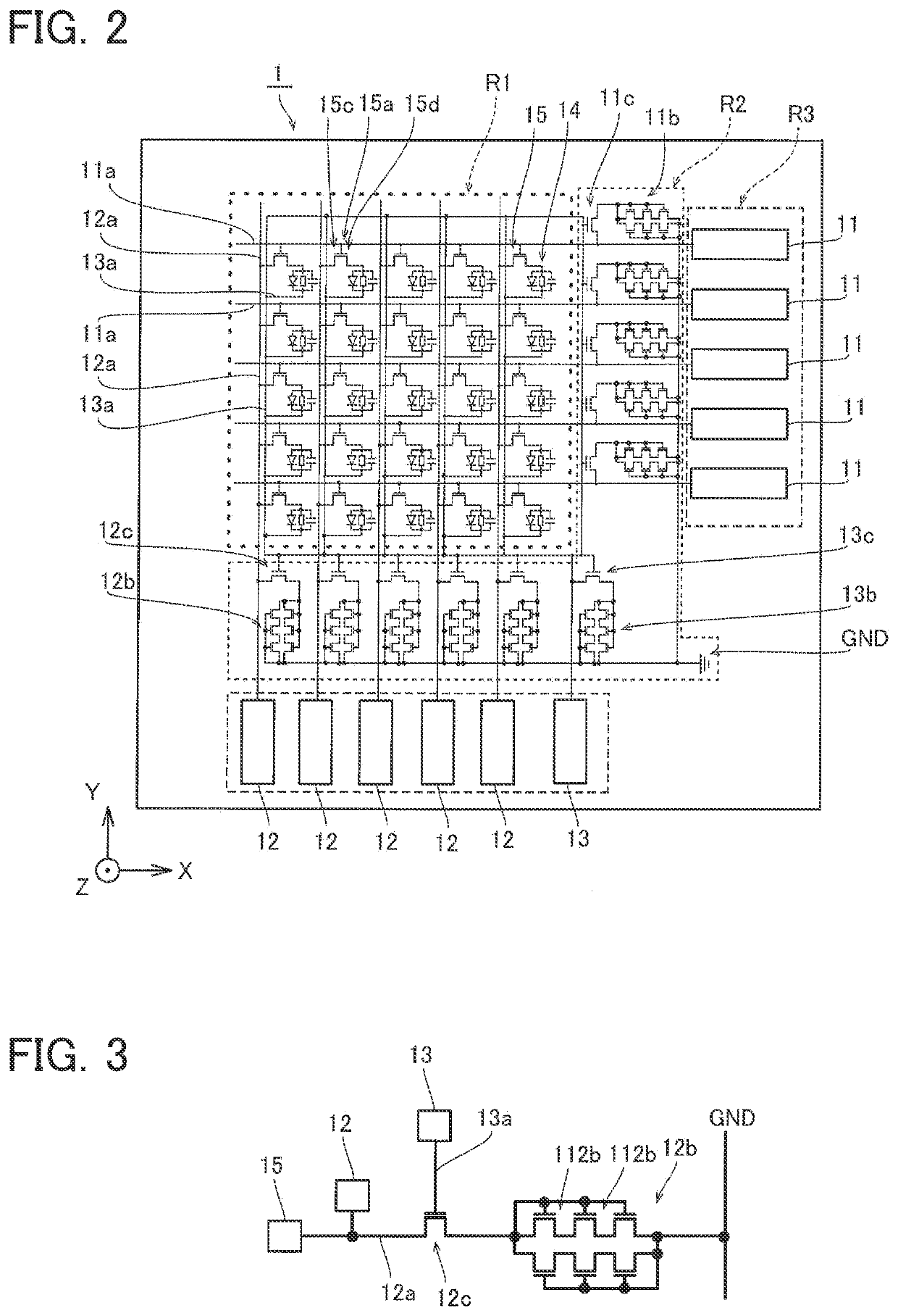
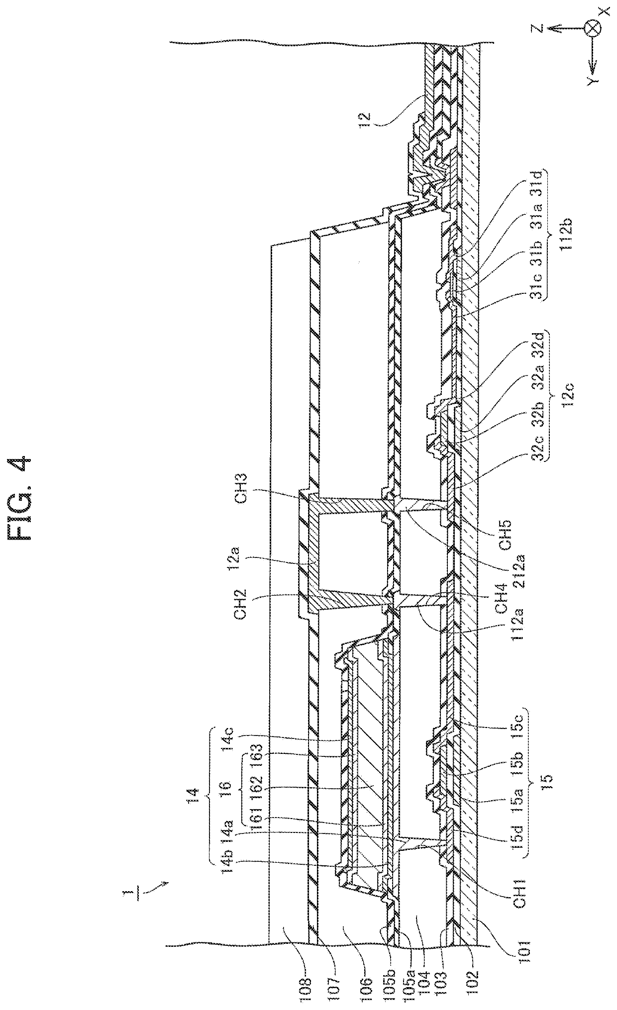
[0013]Described below is an embodiment of the present disclosure, with reference to the drawings. Note that the present disclosure shall not be limited to the embodiment below, and the design presented in the embodiment can be appropriately modified within a scope of the configuration of the present disclosure. Moreover, identical reference signs are used to denote identical or substantially identical components among the drawings. Such components will not be repeatedly elaborated upon. Furthermore, the configurations described in the embodiment and in a modification thereof may be appropriately combined or modified unless otherwise departing from the scope of the present disclosure. For the sake of convenience, the drawings below are simplistically or schematically illustrated. In the drawings, some of the constituent members may be omitted. In addition, the dimensional ratios between the constituent members in the drawings are not necessarily the actual dimensional ratios.

[0014][C...


PUM

PropertyMeasurementUnit
interrupting voltageaaaaaaaaaa
voltageaaaaaaaaaa
semiconductoraaaaaaaaaa

Abstract

A photoelectric conversion panel includes: a substrate; a gate line and a data line formed on the substrate; a pixel transistor connected to the gate line and the data line; a photoelectric conversion element connected to the pixel transistor; an electro-static-discharge protection circuit formed on the substrate and connected to a ground; a depletion transistor for protection connected between either the gate line or the data line and the electro-static-discharge protection circuit; and an interrupting voltage supply line configured to apply an interrupting voltage to a gate electrode of the depletion transistor for protection.

Description

CROSS-REFERENCE TO RELATED APPLICATION[0001]The present application claims priority from Japanese Application JP2021-080249, the content of which is hereby incorporated by reference into this application.BACKGROUND OF THE INVENTION1. Field of the Invention[0002]The present disclosure relates to a photoelectric conversion panel.2. Description of the Related Art[0003]A known photoelectric conversion panel known in the art includes an electro-static-discharge protection circuit. Such a photoelectric conversion panel is disclosed in, for example, Japanese Unexamined Patent Application Publication No. 2009-302092.SUMMARY OF THE INVENTION[0004]The photoelectric conversion panel of a solid-state imaging device according to Japanese Unexamined Patent Application Publication No. 2009-302092 includes a pixel, a scan line, a data line, an electro-static-discharge-protection constant potential line, a bias line, and a protection diode, all of which are formed on a base substrate. This protectio...

Claims


Application Information

Patent Timeline
Patent Type & Authority Applications(United States)
IPC IPC(8): H01L27/146
CPCH01L27/14612H01L27/14603H01L31/115
Inventor TAKITA, RIKIYANAKANO, FUMIKI
Owner SHARP DISPLAY TECH CORP
Why Eureka
Try Eureka