Chain-connected shift register and programmable logic circuit whose logic function is changeable in real time

a shift register and logic function technology, applied in logic circuits using elementary logic circuit components, digital storage, instruments, etc., can solve problems such as difficult to obtain a stable operation in the shift register of the prior-art shift register constructed with such d-type flip-flops, and a relatively large area on the lsi chip

Inactive Publication Date: 2000-01-25
FUJITSU LTD
View PDF3 Cites 178 Cited by
  • Summary
  • Abstract
  • Description
  • Claims
  • Application Information

AI Technical Summary

Problems solved by technology

Therefore, a prior-art shift register constructed with such D-type flip-flops requires a relatively large area on an LSI chip.
There is the following disadvantage in the above-discussed prior-art chain-latch-structure shift register.
When the above-discussed chain-latch-structure shift register is practically constructed, dispersion in operation performance may occur due to performance of the switches constructing the shift register, wire-load capacitance, timing of a supplied clock, etc.
Therefore, it is difficult to obtain a stable operation in that shift register.
Further, in the prior-art programmable logic circuit, there is the following disadvantage.
However, this requirement causes the chip area of the programmable logic circuit to increase.
However, since a driving ability of the N-channel transistor is larger than several times that of the P-channel transistor, a sharp transition may not be obtained at a rising edge of an output waveform of the clock.
Therefore, a number of realizable flip-flops are previously determined, and, thus, it is difficult to further increase the number of flip-flops in the logic cell.

Method used


Image

  • Chain-connected shift register and programmable logic circuit whose logic function is changeable in real time
  • Chain-connected shift register and programmable logic circuit whose logic function is changeable in real time
  • Chain-connected shift register and programmable logic circuit whose logic function is changeable in real time

Examples


second embodiment

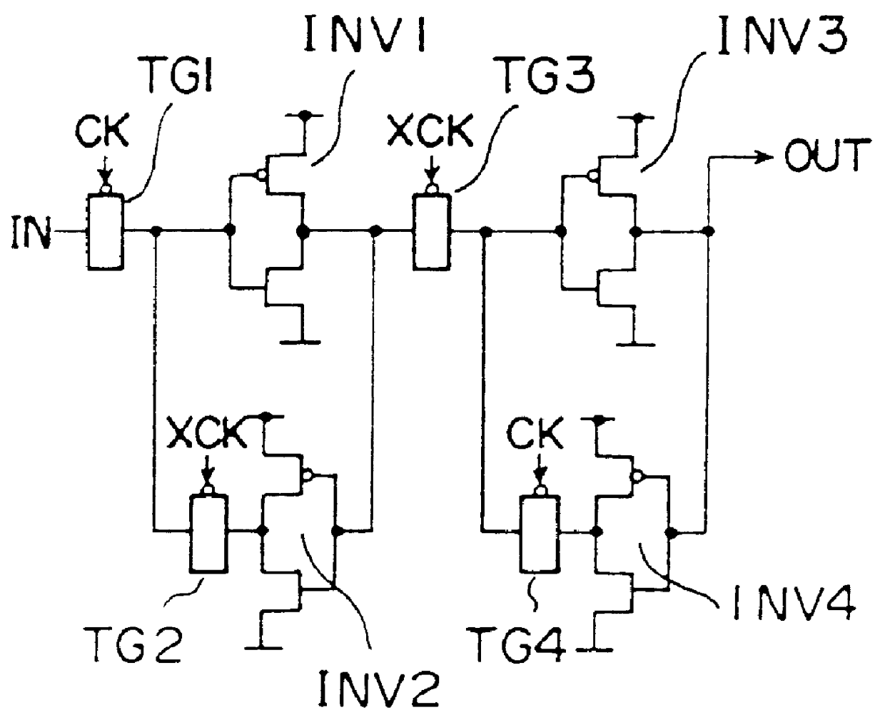
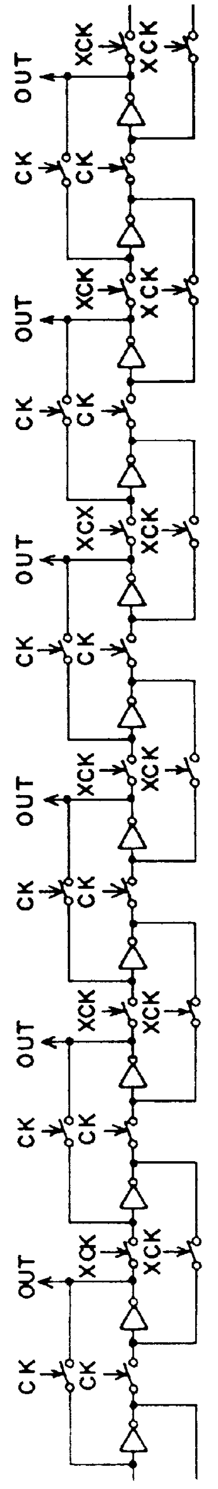
FIG. 19 shows another modification of the shift register according to the present invention shown in FIG. 16. In the shift register shown in FIG. 19, for the switches, the transmission gates and the P-channel MOS transistors are used, and instead of the inverters, NOR gates are used. Also, in the circuit cells b, c, instead of the clock supplying circuit shown in FIG. 6, the clock distributor shown in FIG. 17 is provided.

The clock distributor is provided with the clock signals CK, XCK for the shift register, the clock signals DCK, XDCK for the D-type flip-flop, and the control signals PGM, MODE for selecting one of the two operation modes (shift register and D-type flip-flop modes).

In the shift register shown in FIG. 19, by supplying the given signals to input terminals R, S of the NOR gates, a state of a portion of the shift register may be set to be a desired state. Further, a state of the formed flip-flop may be also set to be a desired state.

Next, a description will be given of ...

first embodiment

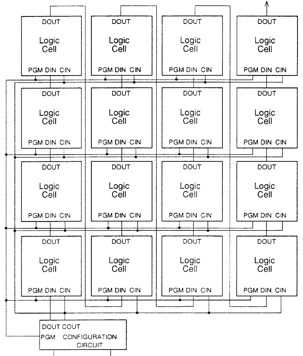
FIG. 20 shows a block diagram of a programmable logic circuit according to the present invention. A logic cell in the programmable logic circuit includes a programmable function unit and a configuration memory for determining a function of the programmable function unit. The programmable function unit may include several flip-flops. The configuration memory is constructed with the shift register shown in FIG. 16. The shift register has circuit cells M0, M1, MFF, M2, M3. The circuit cells M0, M1, M2, M3 respectively have the same circuit configuration as that of the above-discussed circuit cell a. The circuit cell MFF has substantially the same circuit configuration as that of the circuit cell b, c shown in FIG. 16. Therefore, the circuit cell MFF is operable as a flip-flop.

A clock distributor CKD shown in FIG. 20 has substantially the same configuration as that of the clock distributor shown in FIG. 16. The clock distributor CKD is provided with the clocks CK, XCK for the shift regi...


PUM


Abstract

A shift register having a plurality of circuit cells successively connected in a chain formation is proposed. Each of the circuit cells includes a first inversion gate, a first transmission gate, connected to an output of the first inversion gate, being switched by a clock, and a second inversion gate connected to an output of the first transmission gate. The circuit cell further includes a first P-channel transistor, connected between an output of the second inversion gate and an input of the first inversion gate, being switched by the clock, a second transmission gate, connected to the output of the second inversion gate, being switched by an inversion clock, and a second P-channel transistor, connected to the output of the first transmission gate, being switched by the inversion clock. In the shift register, the plurality of circuit cells are successively connected such that the input of the first inversion gate of the circuit cell is connected to an output of a second transmission gate of a former-stage circuit cell, and the output of the first inversion gate of the circuit cell is connected to an output of a second P-channel transistor of the former-stage circuit cell.

Description

1. Field of the InventionThe present invention generally relates to a shift register and a programmable logic circuit, and more particularly, to a chain-connected shift register and a programmable logic circuit using the chainconnected shift register which may be constructed with an extremely small size.The present invention is further directed to a programmable logic circuit and a programmable-logic-circuit system constructed with a plurality of programmable logic circuits, whose logic functions are changeable during a circuit operation. Therefore, a number of realizable logic circuits in the programmable logic circuit may be significantly increased.2. Description of the Related ArtFor a programmable logic circuit, for example, a field programmable gate array (FPGA) is commonly well known. FIG. 1 shows a block diagram of a typical configuration example of the field programmable gate array (FPGA). The FPGA has a plurality of logic cells, each of which may program a desired logic cir...

Claims


Application Information

Patent Timeline
Patent Type & Authority Patents(United States)
IPC IPC(8): G11C19/00G11C19/28H03K19/177
CPCG11C19/00G11C19/28
Inventor AZEGAMI, KENGOYAMASHITA, KOICHI
Owner FUJITSU LTD
Why Eureka
Try Eureka