Check patentability & draft patents in minutes with Patsnap Eureka AI!

Semiconductor memory device

Inactive Publication Date: 2000-03-21
SAMSUNG ELECTRONICS CO LTD
View PDF5 Cites 46 Cited by
  • Summary
  • Abstract
  • Description
  • Claims
  • Application Information

AI Technical Summary

Problems solved by technology

In a hierarchical memory cell array having a sub bit line corresponding to each bank area and a main bit line corresponding to each bank column, generation of one defect (e.g., one defective memory cell) in the memory cell array makes it difficult to read data from other memory cells in the bank area including the defective memory cell.
However, in the case where the redundant circuit system is adopted in the mask ROM operable in the page mode, read of redundant data requires access time to the redundant memory and also the operation time of the switching circuit.
Therefore, when the data read from the redundant memory occurs during page access, the access timing is restricted.
In the case where a non-volatile memory operable in the high-speed access mode such as page mode includes a redundant circuit, delay in data access due to the read of the redundant data and data switching makes it difficult to shorten the access time.

Method used


Image

  • Semiconductor memory device
  • Semiconductor memory device
  • Semiconductor memory device

Examples


example 2

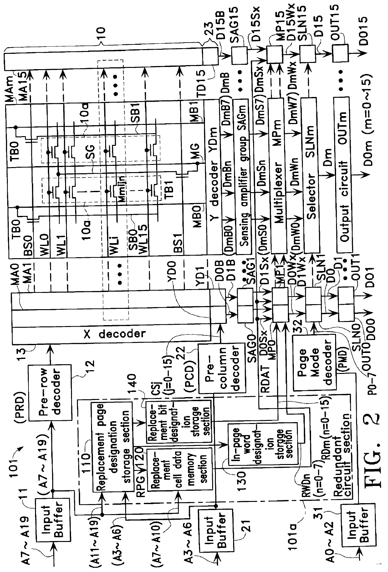
FIG. 10 is a block diagram of a mask ROM as a semiconductor device in a second example according to the present invention, and shows a detailed configuration of a memory cell array included in a main memory of the mask ROM.

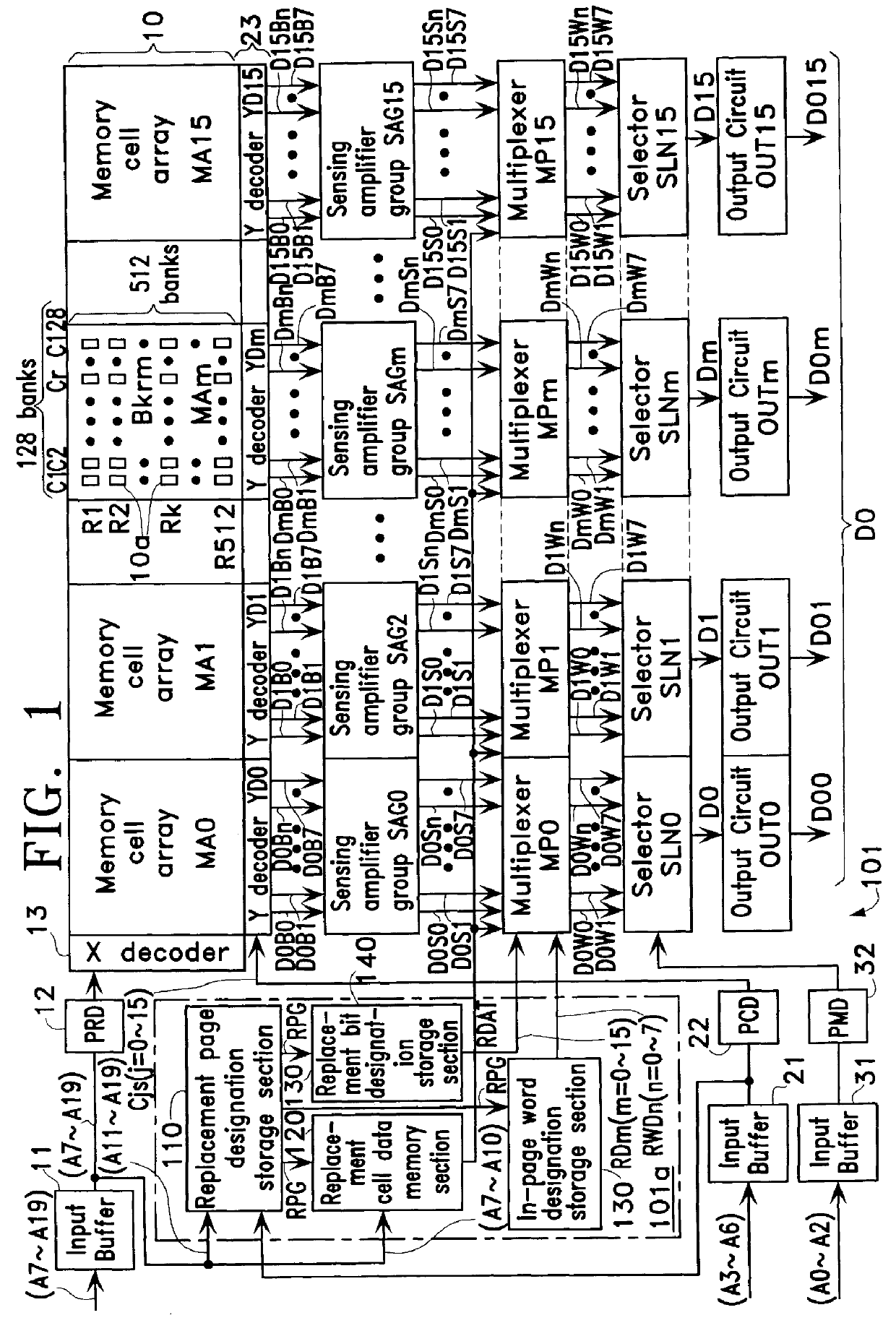
As shown in FIG. 10, a mask ROM 102 operable in a page mode adopting a redundancy compensation system receives an address signal (A0 through A19) and outputs 16-bit output data DO.

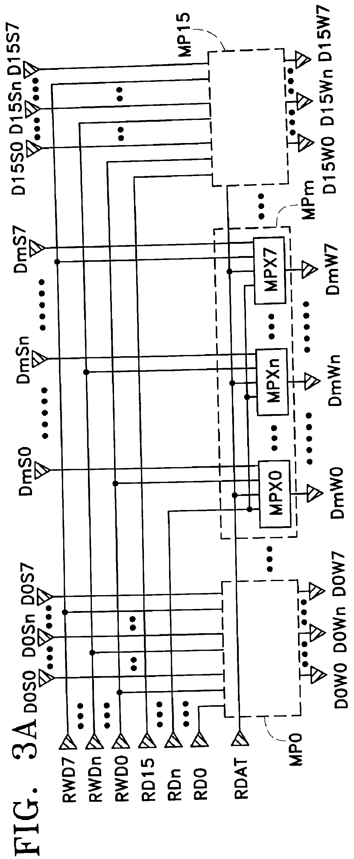
In addition to the redundant circuit section 101a in the mask ROM 101 in the first example, the mask ROM 102 includes a redundant circuit section 102 having the same configuration as that of the redundant circuit section 101a. The redundant circuit section 102 includes storage and memory sections 110, 120, 130 and 140 corresponding to the replacement page designation storage section 110, the replacement cell data memory section 120, the in-page word designation storage section 130 and the replacement bit designation storage section 140. In place of the multiplexers MP0 through MP15, the ...


PUM


Abstract

A semiconductor memory device includes a main memory section, a redundant memory section, a memory cell selection section, a sensing amplification section, a data replacement section, and a data selection section. The redundant memory section includes a replacement cell data memory section for storing replacement cell data to replace cell data in a prescribed memory cell in the main memory section, and a control signal generation section for generating a control signal based on an input address. The memory cell selection section simultaneously selects prescribed cells as a plurality of memory cells corresponding to a prescribed page in the main memory section based on the input address. The sensing amplification section simultaneously senses cell data corresponding to a selected plurality of memory cells as page data. A supply of the replacement cell data and the control signal from the redundant memory section to the data replacement section is performed in a time period from the time when the input address is determined until a time when the page data to be output from the sensing amplification section is determined.

Description

1. Field of the InventionThe present invention relates to a semiconductor memory device, and specifically to a semiconductor memory device having a high-speed read mode adopting a redundancy compensation system, in which data in a defective memory cell is compensated for without delay in access time in the high-speed read mode.2. Description of the Related ArtRecently, as the operation of the microprocessor has become faster, faster-operating semiconductor memory devices have been strongly demanded. While faster usual random access is now being developed on one hand, a semiconductor memory device having a high-speed read mode referred to as the "page mode" is being developed on the other hand as described in, for example, Japanese Laid-Open Publication No. 8-63990.In the page-mode read operation, a plurality of memory cells, the number of which corresponds to a plurality of addresses in the memory cell arrays in accordance with the column address and the row address in an input addr...

Claims


Application Information

Patent Timeline
IPC IPC(8): G11C29/00G11C16/06G11C7/00G11C29/04
CPCG11C7/1012G11C29/70G11C17/00
Inventor HOTTA, YASUHIROKOUCHI, SHUICHIRO
Owner SAMSUNG ELECTRONICS CO LTD
Features
  • R&D
  • Intellectual Property
  • Life Sciences
  • Materials
  • Tech Scout
  • Unparalleled Data Quality
  • Higher Quality Content
  • 60% Fewer Hallucinations
Learn More