
Optical waveguide device for connections without optical axis adjustment

a technology of optical waveguide and connection, applied in the direction of optics, optical elements, instruments, etc., can solve the problems of increasing the production cost of optical devices, difficult to precisely control the dimensional accuracy at the level of several micrometers, and difficult application of these optical parts

Inactive Publication Date: 2000-04-18
MITSUBISHI GAS CHEM CO INC
View PDF9 Cites 80 Cited by
  • Summary
  • Abstract
  • Description
  • Claims
  • Application Information

AI Technical Summary

Problems solved by technology

In particular, at present, the application of these optical parts is considered difficult in many cases since they are expensive.
Of the above steps, the optical axes adjustment step of adjusting the relative positions of the optical waveguide part and the optical fiber array to optimum positions and joining these two to each other, i.e., the axial alignment step, requires measuring instruments such as an optical stage, a light source and an optical power meter, a long period of time and a large volume of labor, and this step is the greatest factor that increases the production cost of the optical devices.
In the conventional method, however, the film shrinks approximately by 3 or 4% when the formed film is separated from the container, and it is therefore difficult to precisely control the dimensional accuracy at the level of several micrometers.
When the adhesion between the glass substrate and the polymer film is poor, the polymer film may peel off from the glass substrate during a period from the formation of the polymer film to the post processing.

Method used


Image

  • Optical waveguide device for connections without optical axis adjustment
  • Optical waveguide device for connections without optical axis adjustment
  • Optical waveguide device for connections without optical axis adjustment

Examples


example 1 (

8.times.8 optical star coupler device for 50 .mu.m optical fiber)

(Photo-mask)

A photo-mask having a size of 127 mm.times.127 mm and having a pattern shown in FIG. 4 was used.

The optical circuit of the photo-mask had a 8.times.8 branched waveguide pattern in which each waveguide in an end portion had a width of 40 .mu.m and the pitch from a waveguide to an adjacent one was 250 .mu.m. The detail thereof was as shown in FIG. 5.

(Pretreatment of glass substrate)

For improving the adhesion between a film to be formed and a glass substrate (c), a groove having a width of 0.5 mm and a depth of 0.7 mm was made on a glass substrate having a 15.times.15 cm size and a thickness of 1.1 mm in those portions which were 2 cm inside from four sides and were on sides of an 11 cm.times.11 cm area, with a dicing machine, to form a peel preventer.

(Fabrication of optical waveguide)

Predetermined amounts of a polycarbonate resin (Iupilon Z, supplied by Mitsubishi Gas Chemical Co., Inc.) synthesized from bisp...


PUM

PropertyMeasurementUnit
Electric potential / voltageaaaaaaaaaa
Fractionaaaaaaaaaa
Fractionaaaaaaaaaa

Abstract

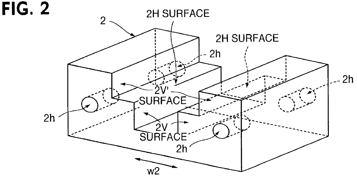
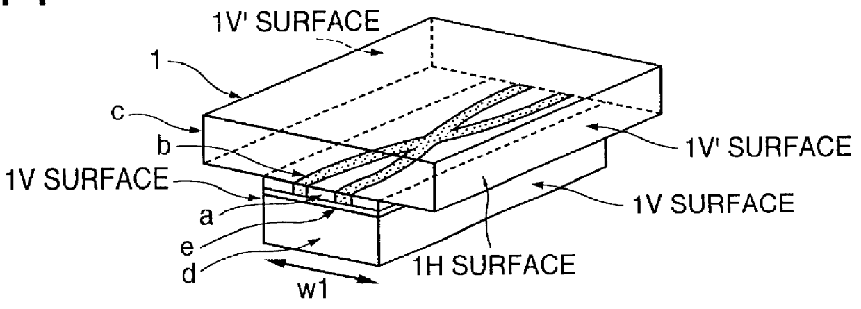
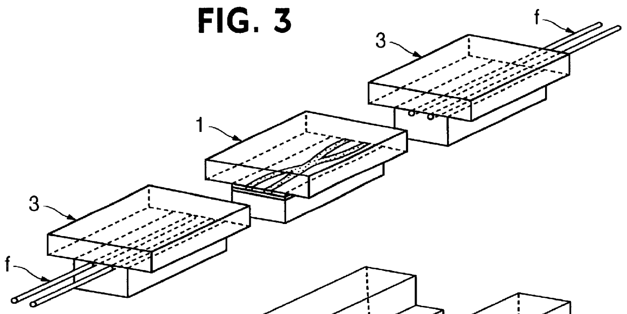
An optical device which can be fabricated without any axial alignment by optical measurement and can therefore be produced at a remarkably decreased cost, and which is composed of an optical waveguide part (1) obtained by perpendicularly cutting an optically-transparent polymer film having a glass substrate attached thereto and having a refractive index distribution formed, in a predetermined position measured from the position of the refractive index distribution as a reference, and a holder part (2) for holding the optical waveguide part (1) in a predetermined position, the holder part (2) having a horizontal guide surface (2H) and a vertical guide surface (2V), the optical waveguide part (1) having a glass substrate surface or a polymer film surface coherently attached to the horizontal guide surface (2H) of the holder part (2), and the optical waveguide part (1) having a perpendicularly cut surface coherently attached to the vertical guide surface (2V) of the holder part (2).

Description

The present invention relates to the structure of an optical waveguide type optical device for use in an optical branching and coupling device and an optical receiver and transmitter module. More specifically, it relates to an optical device connectable with an optical fiber array without optical axis adjustment based on optical measurement.PRIOR ARTThe application of optical parts such as an optical branching and coupling device and an optical receiver and transmitter module is rapidly broadening in use range with broadening fields of telecommunication, data processing and image processing. It is therefore being demanded to improve their performance and decrease their price. In particular, at present, the application of these optical parts is considered difficult in many cases since they are expensive. For increasing the use thereof in the future, it is considered the most important key to decrease their production costs for decreasing their prices.For example, the production steps...

Claims


Application Information

Patent Timeline
IPC IPC(8): G02B6/122G02B6/30G02B6/42C08F283/02G02B1/04
CPCG02B6/1221G02B6/30G02B6/4233G02B6/423
Inventor TAKANO, TOSHIHIROOHBA, MICHIOKAWABATA, YASUNARI
Owner MITSUBISHI GAS CHEM CO INC
Learn More