

Treatment device
- Summary
- Abstract
- Description
- Claims
- Application Information
AI Technical Summary
Benefits of technology
Problems solved by technology
Method used
Image

Examples
first embodiment
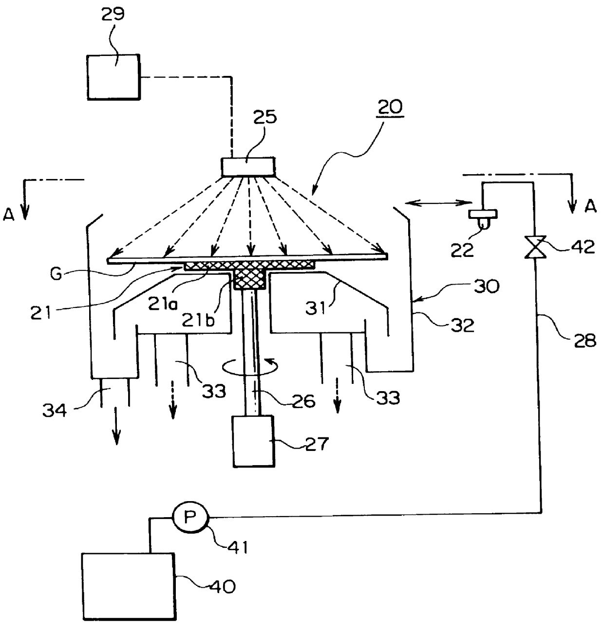
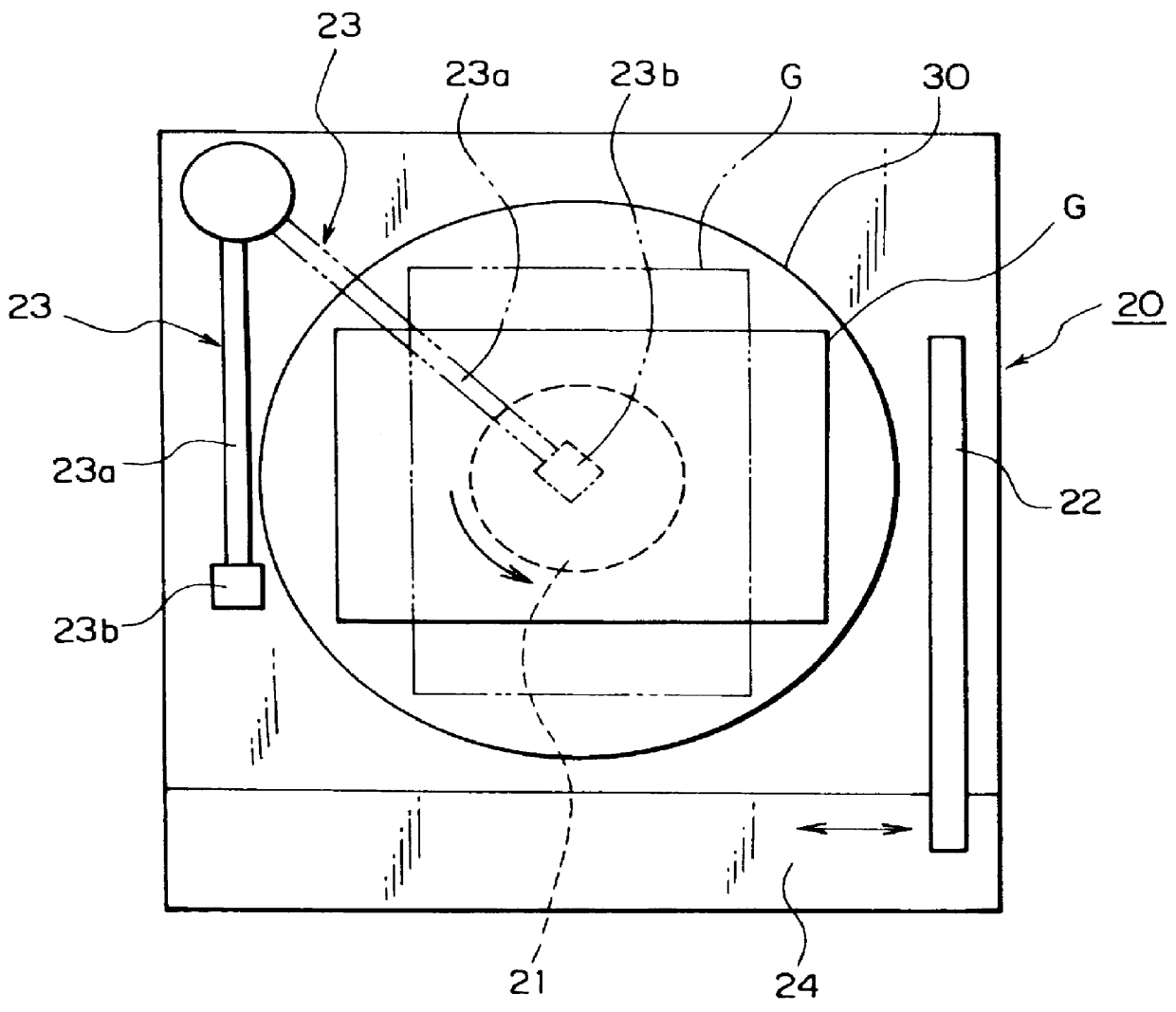
As shown in FIGS. 2 and 3, the developing device 20 comprises a spin chuck 21 rotatable horizontally and serving as a holding means for holding the substrate G by vacuum sucking; a container 30 containing the spin chuck 21 and the substrate G; a developing solution supply nozzle 22 (treating solution supply means) for supplying the developing solution to the resist film formed on the surface of the substrate G; a cleaning liquid supply nozzle 23 for supplying the rinsing liquid (cleaning solution) to the circuit pattern formed on the surface of the developed substrate G; a moving mechanism 24 for moving the developing solution supply nozzle 22 between a waiting position set at the right side in FIG. 3 and a treating position located above the substrate G; and an ionizer (destaticizing fluid supply means) 25 located at an upper position of the spin chuck 21 and spraying a destaticizing fluid, for example, an ionized gas to the substrate G and the spin chuck 21. The operation of the i...
second embodiment
FIG. 6 is a sectional view showing a second embodiment of the treatment device of the present invention. FIG. 7 is a sectional view showing main portions of the treatment device.
In the second embodiment, a destaticizing fluid is supplied from a position located below the spin chuck 21 to destaticize the spin chuck 21 and the substrate G which have been charged. That is, a pure water supply nozzle 50 (destaticizing fluid supply means) which jets the destaticizing fluid, for example, pure water to the spin chuck 21 and the substrate G is installed on the lower container 31 positioned below the spin chuck 21 to destaticize the spin chuck 21 and the substrate G which have teen charged. A controller 59 controls the pure water-jetting timing.
FIG. 8 shows the control system of the controller 59. The pure water supplied from a pure water supply source 50a is supplied to the spin chuck 21 and the substrate G from the pure water supply nozzle 50 through a valve 50b. Nitrogen gas supplied from...
example 1
k made of polyphenylene sulfide (see FIG. 5A)
Diameter D of substrate-placing portion 21a=300 mm.phi.; thickness H thereof=9 mm; diameter d of boss 21b=300 mm.phi.; thickness h thereof=30 mm
PUM
 Abstract
Description
Claims
Application Information