Active matrix display device having defect repair extension line beneath each pixel

a display device and active matrix technology, applied in the field of display devices, can solve the problems of two line defects on the display, point defects or line defects of the resultant display device, and display device defects found to be defectiv

Inactive Publication Date: 2000-06-06
SHARP KK
View PDF29 Cites 29 Cited by
  • Summary
  • Abstract
  • Description
  • Claims
  • Application Information

AI Technical Summary

Problems solved by technology

Such leakage may bring about a point defect or a line defect of the resultant display device.
This leakage results in two line defects on the display.
If a display panel with these defects is used to complete a display device, the resultant displayed device is found to be defective.
This lowers production yield.
Repair of this type of leakage is considerably difficult because no point defect as a mark for leakage repair is exhibited.
Though it is not impossible to locate a leak portion by scanning along the source bus line 1112a or 1112b with a microscope, it requires an enormous amount of time.
This type of leakage may occur more significantly when pixel electrodes and source bus lines are formed in different layers with an insulating film therebetween.
Especially, this leakage may occur when a transparent conductive film such as an ITO film is used as source bus lines.

Method used


Image

  • Active matrix display device having defect repair extension line beneath each pixel
  • Active matrix display device having defect repair extension line beneath each pixel
  • Active matrix display device having defect repair extension line beneath each pixel

Examples


example 2

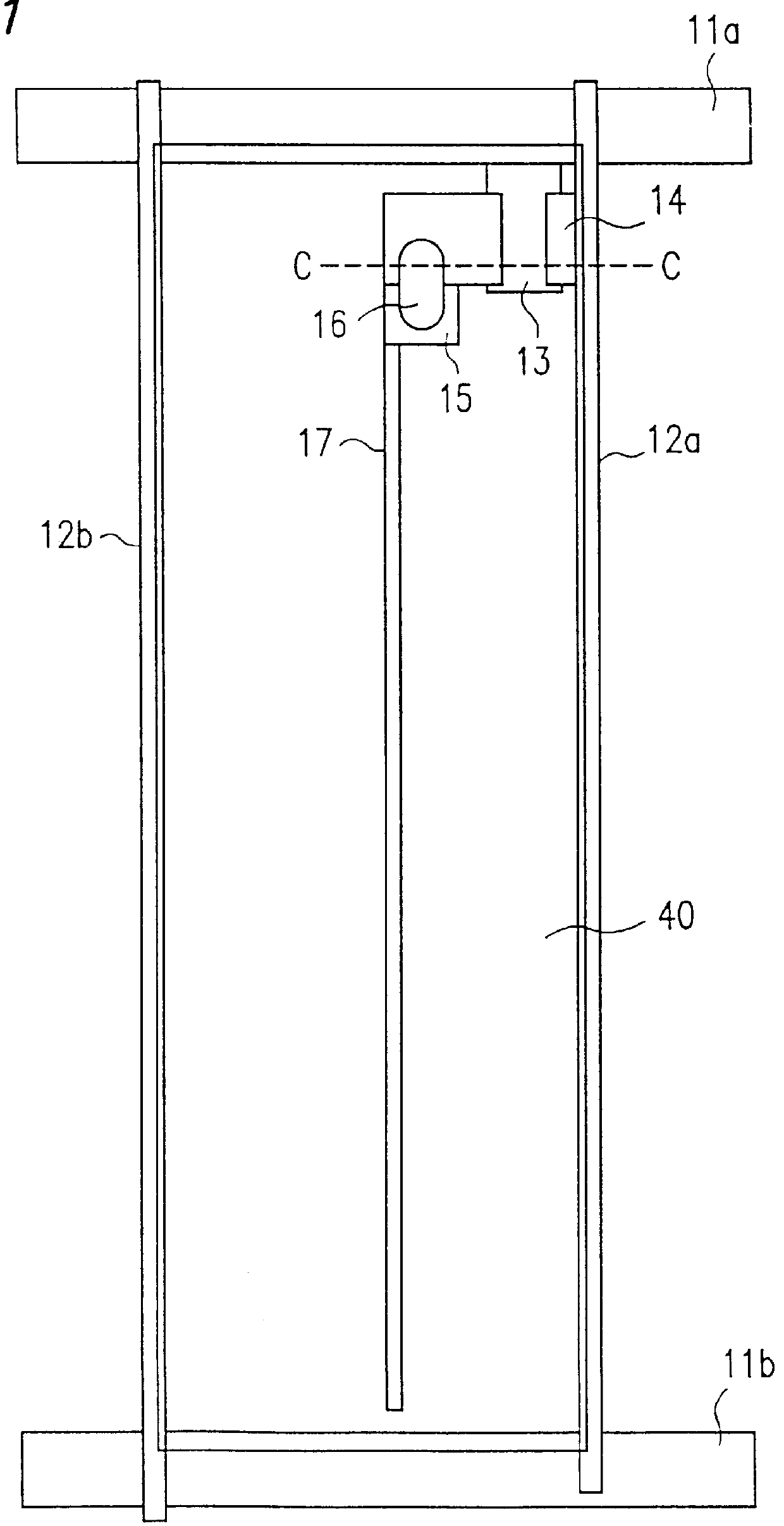
FIG. 7 is a plan view of one pixel of an active matrix display device of Example 2 according to the present invention. FIGS. 8 and 9 are sectional views taken along line B--B and line D--D of FIG. 7, respectively.

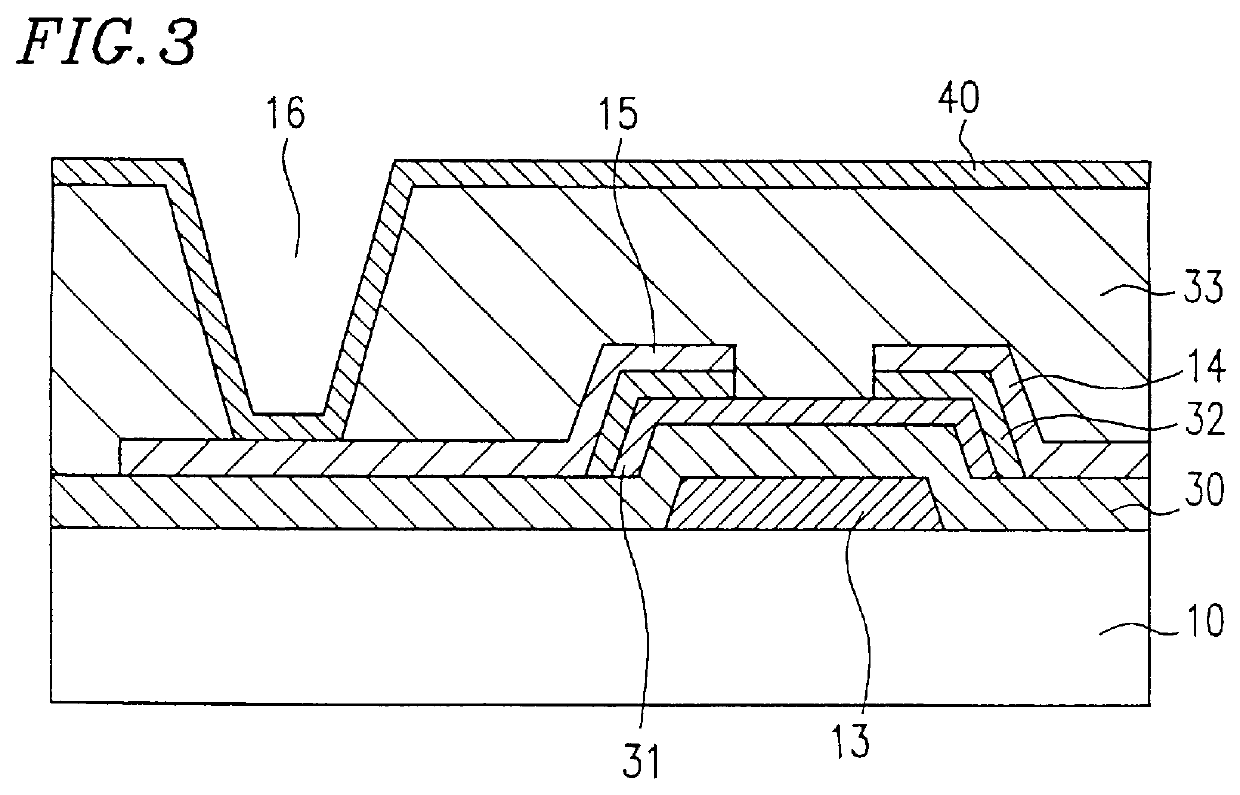
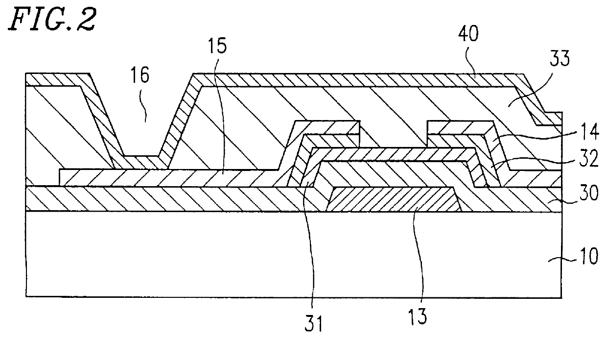
In Example 1, the contact hole 16 was formed through the insulating layer 33 above the drain electrode 15. In this configuration, however, the size of the contact hole 16 is restricted for the following reason. That is, if a larger contact hole is desired, the drain electrode 15 must be larger. As the drain electrode 15 is larger, the aperture ratio of the device becomes lower.

In order to overcome the above problem, the active matrix display device of this example is fabricated in the following manner. First, a layer of a conductive material is deposited on a substrate 110, such as a glass substrate, and is patterned to form a plurality of gate bus lines 111 which extend in parallel and each of which has a plurality of projections 113 serving as gate electrodes of TFTs. The...

example 3

FIG. 10 is a plan view of one pixel of an active matrix display device of Example 3 according to the present invention. FIG. 11 is a sectional view taken along line E--E of FIG. 10. In FIG. 10, a pixel electrode is not shown for simplification.

A display device is generally provided with a storage capacitor in parallel with each pixel electrode to improve the charge holding property. In this example, in order to provide such a storage capacitor, a storage capacitor bus line 318 is formed on a substrate 310, such as a glass substrate, by patterning a conductive material simultaneously with the formation of gate bus lines 311a and 311b of the same conductive material in parallel with the gate bus lines 311a and 311b. The potential of the storage capacitor bus line 318 is made equal to that of a counter electrode (not shown) (Cs-on-Common method).

In this example, the gate bus lines 311a and 311b having projections 313 serving as gate electrodes of TFTs, the source bus lines 312 having p...

example 4

FIG. 14 is a plan view of one pixel of an active matrix display device of Example 4 according to the present invention. The configuration of the active matrix display device of this example is the same as that of Example 3 shown in FIG. 10 except that source bus lines 512a and 512b are formed of a transparent conductive material used for the formation of a contact portion 539. Therefore, gate bus lines 511 having projections 513, storage capacitor bus lines 518, the source bus lines 512a and 512b having projections 514 serving as source electrodes, drain electrodes 515, contact portions 539 and antenna lines 517 are formed in a manner similar to that in Example 3. Thus, due to provision of the antennal lines 517, the same effects as those described in Example 1 are also obtained.

In this example, a conductive pattern piece 520 which brings about leakage between the source bus lines 512a and 512b is also transparent. Accordingly, it is difficult to locate a leakage position with an mi...


PUM

PropertyMeasurementUnit
thicknessaaaaaaaaaa
thicknessaaaaaaaaaa
thicknessaaaaaaaaaa

Abstract

The active matrix display device of this invention includes: a substrate and a scanning line running in a first direction formed in a first layer located above the substrate. The display device also includes a signal line running in a second direction formed in a second layer located above the substrate; a switching element connected with the scanning line and the signal line; an insulating film formed above the scanning line, the signal line, and the switching element; and a pixel electrode formed above the insulating film so as to connect with the switching element, wherein the active matrix display device further comprises an extension line connected with an electrode of the switching element, the extension line being formed in the second layer so as not to intersect the signal line.

Description

1. Field of the InventionThe present invention relates to a display device where display is effected by applying a driving signal to a pixel electrode via a switching element. More specifically, the present invention relates to an active matrix display device where high-density display is effected by arranging pixel electrodes in a matrix.2. Description of the Related ArtDisplay devices such as a liquid crystal display device, an EL (electroluminescence) display device, and a plasma display device are conventionally operated by methods where a display pattern is formed on a screen by selecting desired pixels among a plurality of pixels arranged in a matrix. As one of such methods, an active matrix driving method is known.In the active matrix driving method, pixel electrodes arranged in a matrix are independently driven by controlling switching elements connected to the respective pixel electrodes. Such an active matrix driving method realizes high contrast display and thus has been ...

Claims


Application Information

Patent Timeline
Patent Type & Authority Patents(United States)
IPC IPC(8): G02F1/13G02F1/1362G01R31/00G02F1/133G02F1/136G02F1/1368G09F9/30
CPCG02F1/1362G02F1/136286G02F2001/136263G02F1/136259G02F1/136263G02F1/1309G02F1/13454
Inventor KANEMORI, YUZURUBAN, ATSUSHIKATAYAMA, MIKIO
Owner SHARP KK
Why Eureka
Try Eureka