Method, system and apparatus for aggregating failures across multiple memories and applying a common defect repair solution to all of the multiple memories

a technology of multiple memory and defect repair, applied in the field of integrated circuits, can solve the problems of large amount of die size consumed by bist circuits and associated circuitry, increase the complexity and density of circuit devices formed within a single integrated circuit (ic), and increase the complexity of circuit devices formed within a single integrated circuit (ic). the effect of reducing the area devoted to the integrated circui

Active Publication Date: 2006-01-31
TWITTER INC
View PDF17 Cites 25 Cited by
  • Summary
  • Abstract
  • Description
  • Claims
  • Application Information

AI Technical Summary

Benefits of technology

[0008]The present invention introduces an improved integrated circuit and associated BIST testing and repair methodology that minimize integrated circui

Problems solved by technology

As integrated circuit technology has advanced, the complexity and density of circuit devices formed within a single integrated circuit (IC) has increased dramatically.
Consequently, several problems have arisen with regard to

Method used


Image

  • Method, system and apparatus for aggregating failures across multiple memories and applying a common defect repair solution to all of the multiple memories
  • Method, system and apparatus for aggregating failures across multiple memories and applying a common defect repair solution to all of the multiple memories
  • Method, system and apparatus for aggregating failures across multiple memories and applying a common defect repair solution to all of the multiple memories

Examples


Embodiment Construction

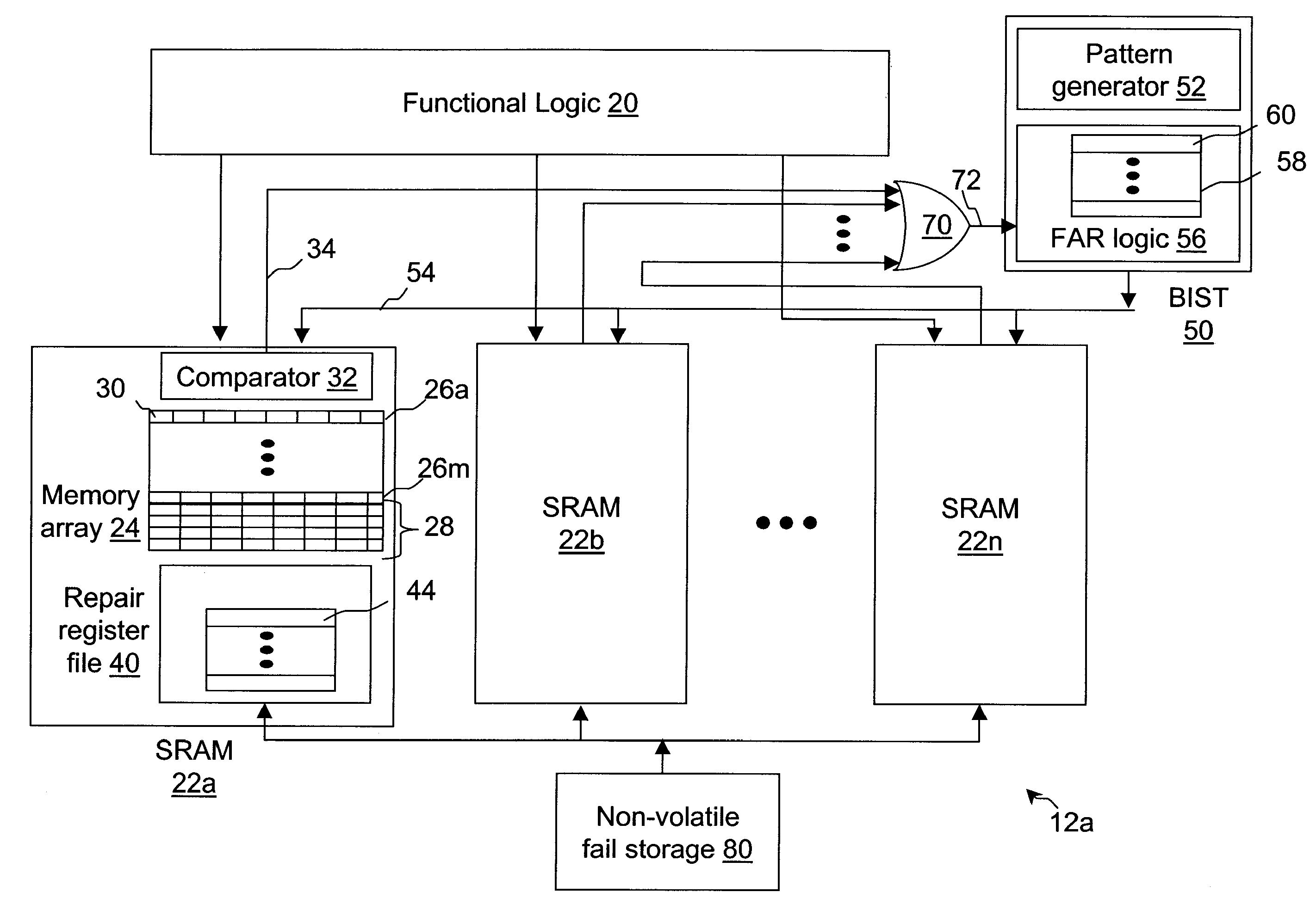
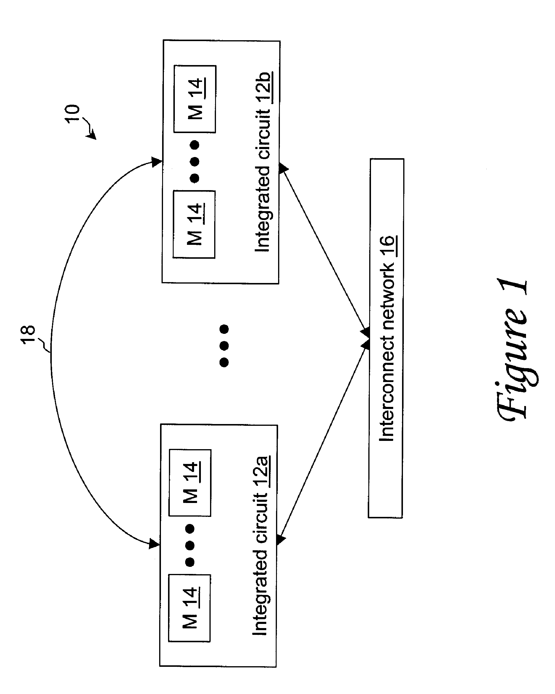
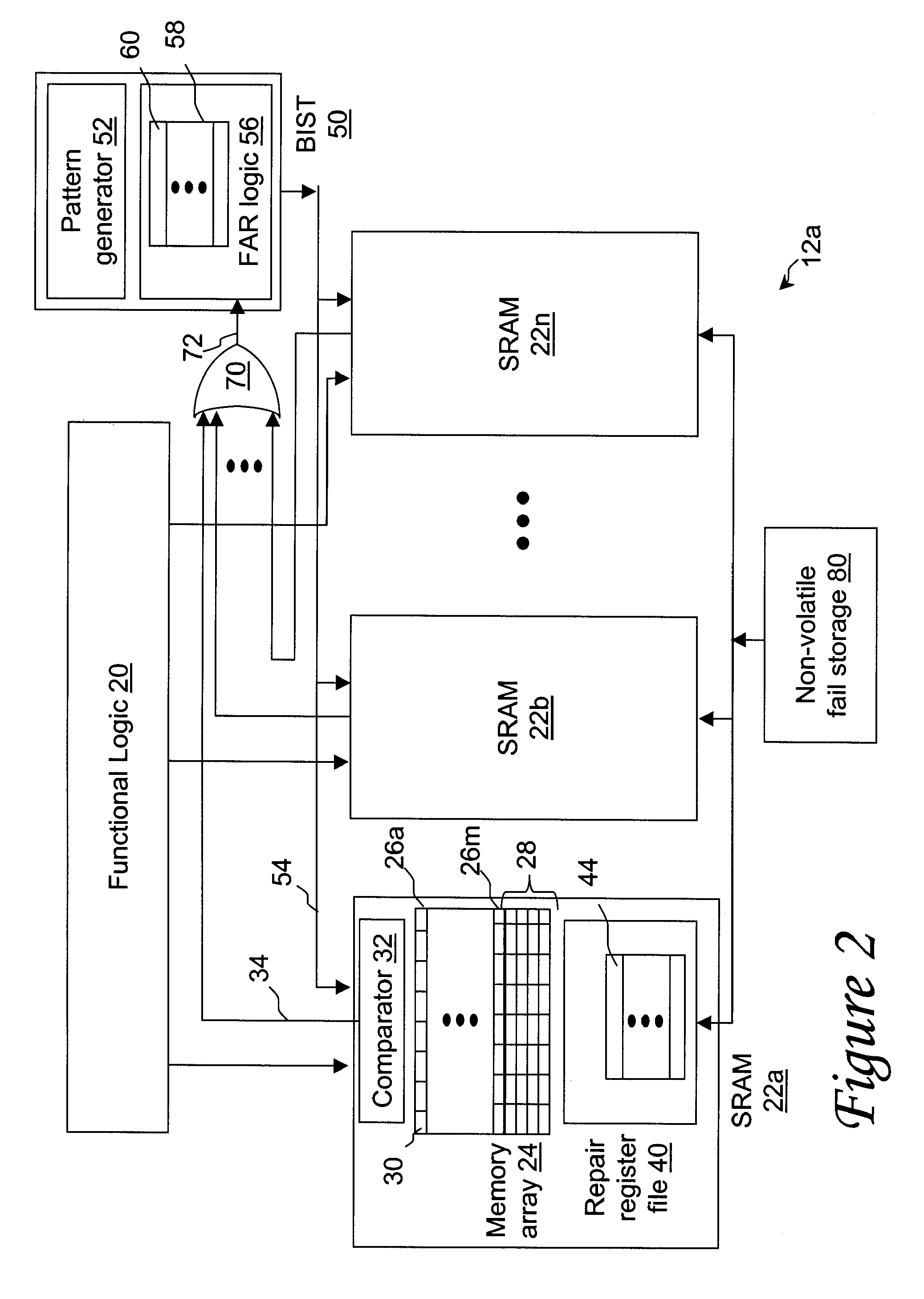
[0017]With reference now to the figures and, in particular, with reference to FIG. 1, there is illustrated a high-level block diagram of an electronic system in accordance with the present invention. Electronic system 10 may comprise, for example, a computer system, a network device, an electronic appliance, or any of a myriad of other well-known or future developed electronic systems containing integrated circuitry.

[0018]As shown, electronic system 10 includes multiple integrated circuit chips 12, which are interconnected for communication through direct connections 18 and / or an interconnect network 16. In various embodiments of electronic system 10, direct connections 18 and interconnect network 16 may comprise, for example, metal wiring or traces, buses, switches, cabling, and / or wireless radio frequency or infrared communication links, and the like.

[0019]At least one and possibly numerous integrated circuits 12 include multiple memories (M) 14 for storing data. Memories 14 may b...


PUM


Abstract

An integrated circuit includes a plurality of separate memory arrays each having a respective one of a plurality of inputs and a respective one of a plurality of outputs. Each output provides an output value indicative of whether a storage location associated with an applied address is passing or failing. The integrated circuit further includes a shared built-in self-test (BIST) and repair system coupled to all of the plurality of inputs and all of the plurality of outputs. The shared BIST and repair system applies addresses and data to the plurality of inputs to test the plurality of memory arrays for failing storage locations. In response to detection of a failing storage location in any of the plurality of memory arrays, the shared BIST and repair system applies a common address remapping to all of the plurality of memory arrays to remap, in each memory array, the address associated with the failing storage location to a different storage location

Description

BACKGROUND OF INVENTION[0001]1. Technical Field[0002]The present invention relates in general to integrated circuitry and, in particular, to integrated circuits including multiple memory arrays. Still more particularly, the present invention relates to the aggregation of detected failures across multiple memory arrays and the application of a common repair solution to all of the multiple memory arrays.[0003]2. Description of the Related Art[0004]As integrated circuit technology has advanced, the complexity and density of circuit devices formed within a single integrated circuit (IC) has increased dramatically. Consequently, several problems have arisen with regard to testing ICs. For example, while the conventional methodology for testing a memory array within an IC may be relatively straight forward,[0005]ICs typically have far fewer I / O pins available to an external circuit tester than are required to adequately test the memory array.[0006]A general solution to the above-described...

Claims


Application Information

Patent Timeline
IPC IPC(8): G11C29/00G06F11/00G01R31/28G11C29/44
CPCG11C29/44G11C29/4401G11C29/802G11C29/806G11C2029/0401G11C29/789
Inventor OUELLETTE, MICHAEL R.TELLEZ, GUSTAVO ENRIQUEZUCHOWSKI, PAUL STEVEN
Owner TWITTER INC
Why Eureka
Try Eureka