

Output stage interface circuit for outputting digital data onto a data bus
a technology of digital data and interface circuit, which is applied in the direction of logic circuits, oscillator generator details, electric pulse generator details, etc., can solve the problems of undesirable quadrupling of die area required by the interface circuit of thurber, and achieve the effect of minimising the die area required for the interface circuit according to the invention
- Summary
- Abstract
- Description
- Claims
- Application Information
AI Technical Summary
Benefits of technology
Problems solved by technology
Method used
Image

Examples
Embodiment Construction
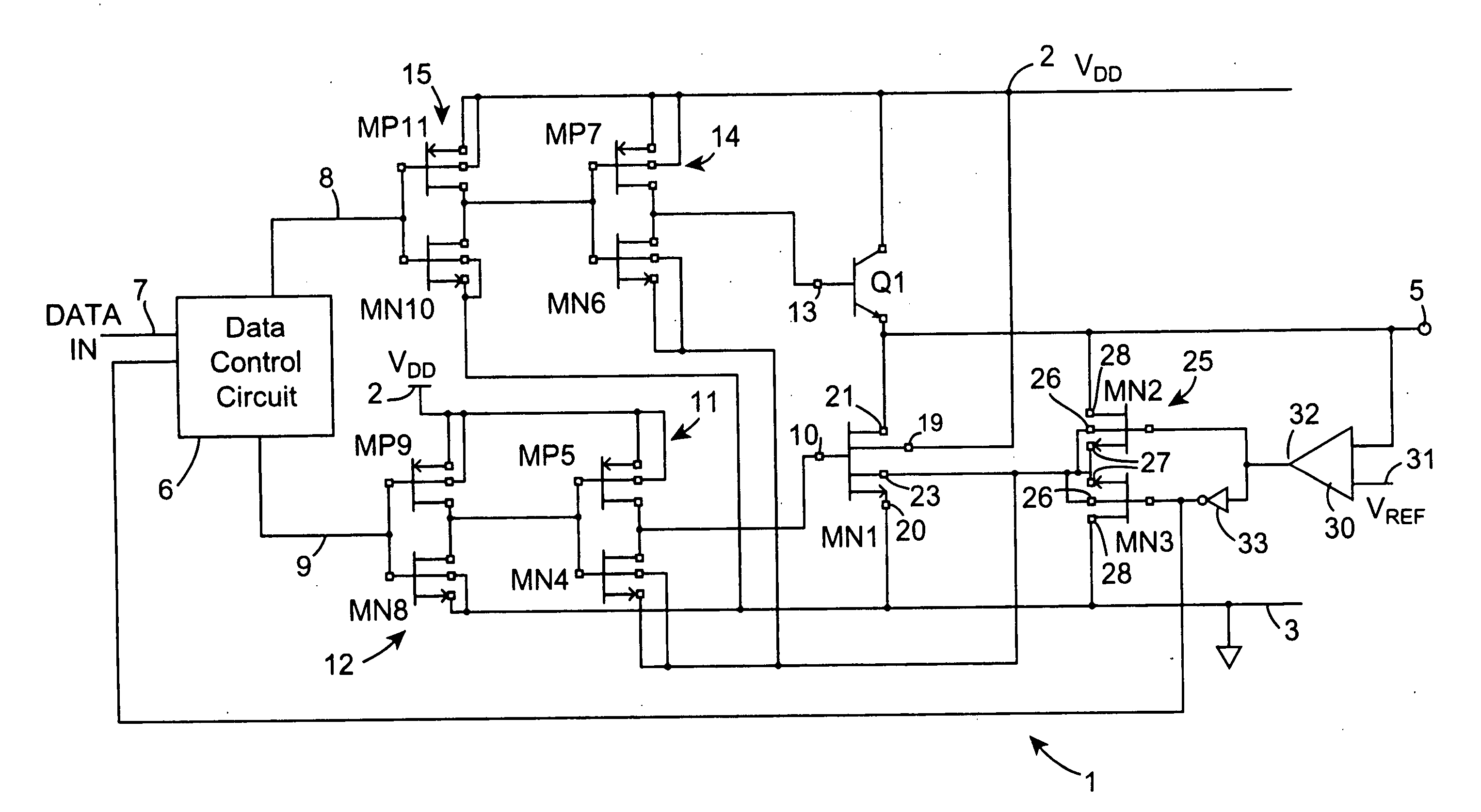
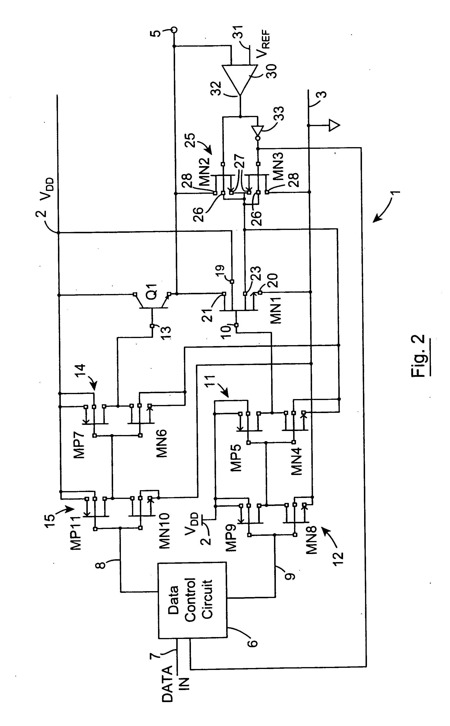
[0047] Referring to the drawings and initially to FIGS. 2 and 3 thereof, there is illustrated an output stage interface circuit according to the invention, indicated generally by the reference numeral 1, for interfacing a digital data processing device (not shown) with a shared data bus (also not shown) for outputting digital data from the data processing device onto the data bus. The data bus typically would be a shared data bus which would operate to a transmission standard, which permitted a relatively wide operating voltage range, typically, down to at least −7 volts, and up to at least +12 volts. The data processing device may be any type of data processing device, for example, a computer, in particular a laptop computer, or any other such digital data processing device or circuit, which in particular, is of the type which operates with relatively low voltage power supply, typically, a +3 volts power supply. In this embodiment of the invention the interface circuit 1 is impleme...
PUM
 Abstract
Description
Claims
Application Information