

Field programmable gate array having internal logic transistors with two different gate insulator thicknesses
a logic transistor and gate insulator technology, applied in the field of field programmable gate arrays having internal logic transistors with two, can solve the problems of high undesirable standby current drain, undesirable power current spike, damage to fpga and/or clamp,
- Summary
- Abstract
- Description
- Claims
- Application Information
AI Technical Summary
Problems solved by technology
Method used
Image

Examples
example 2
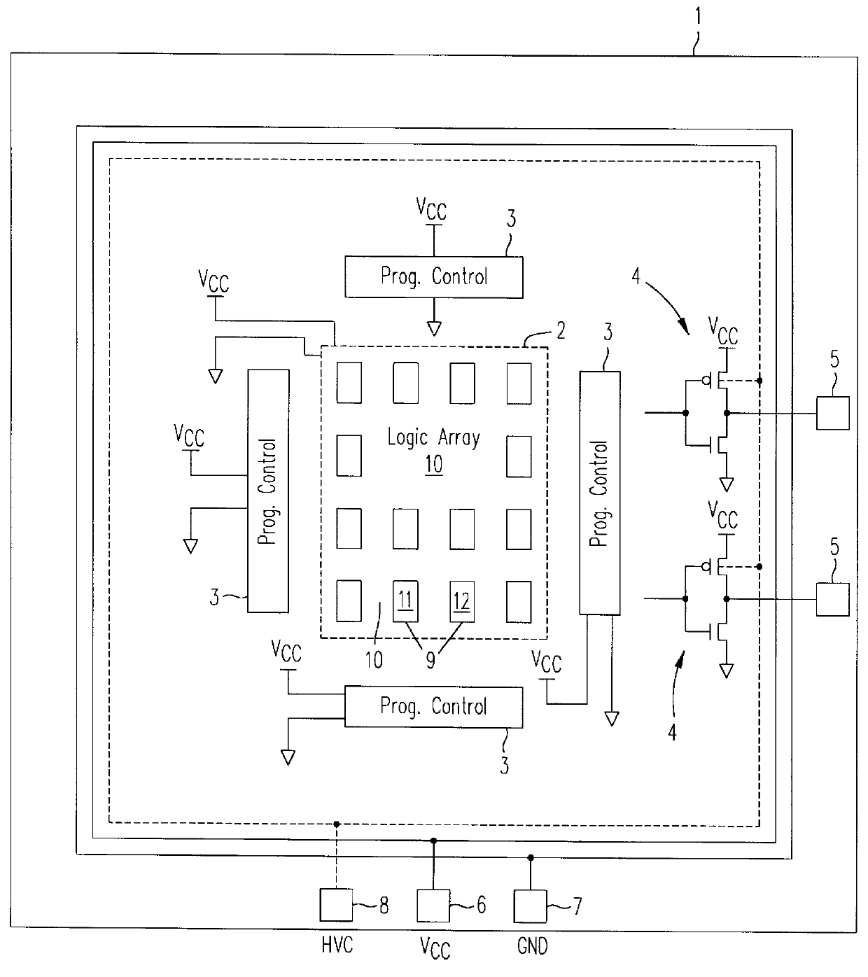
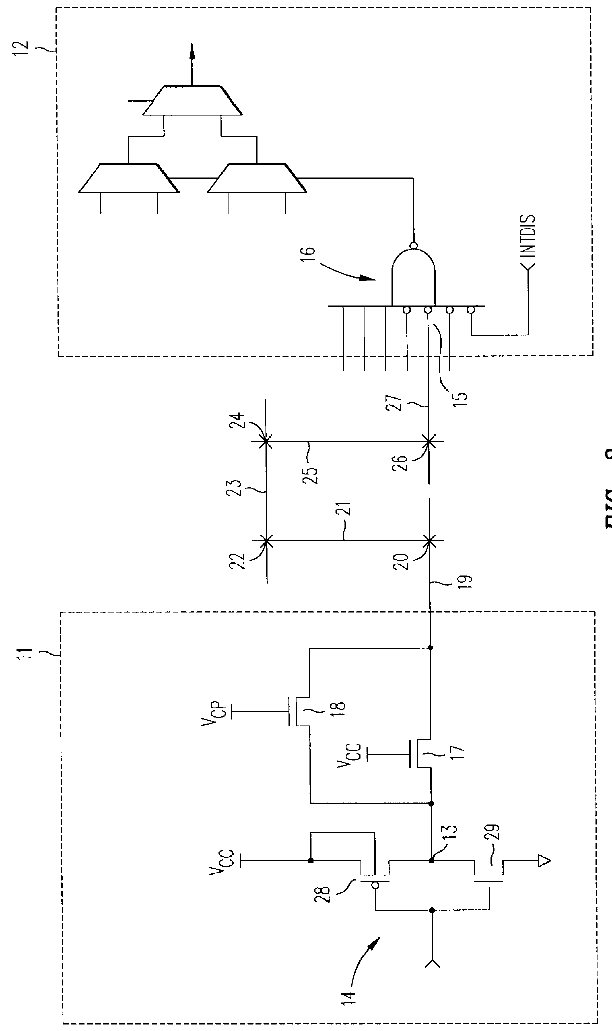
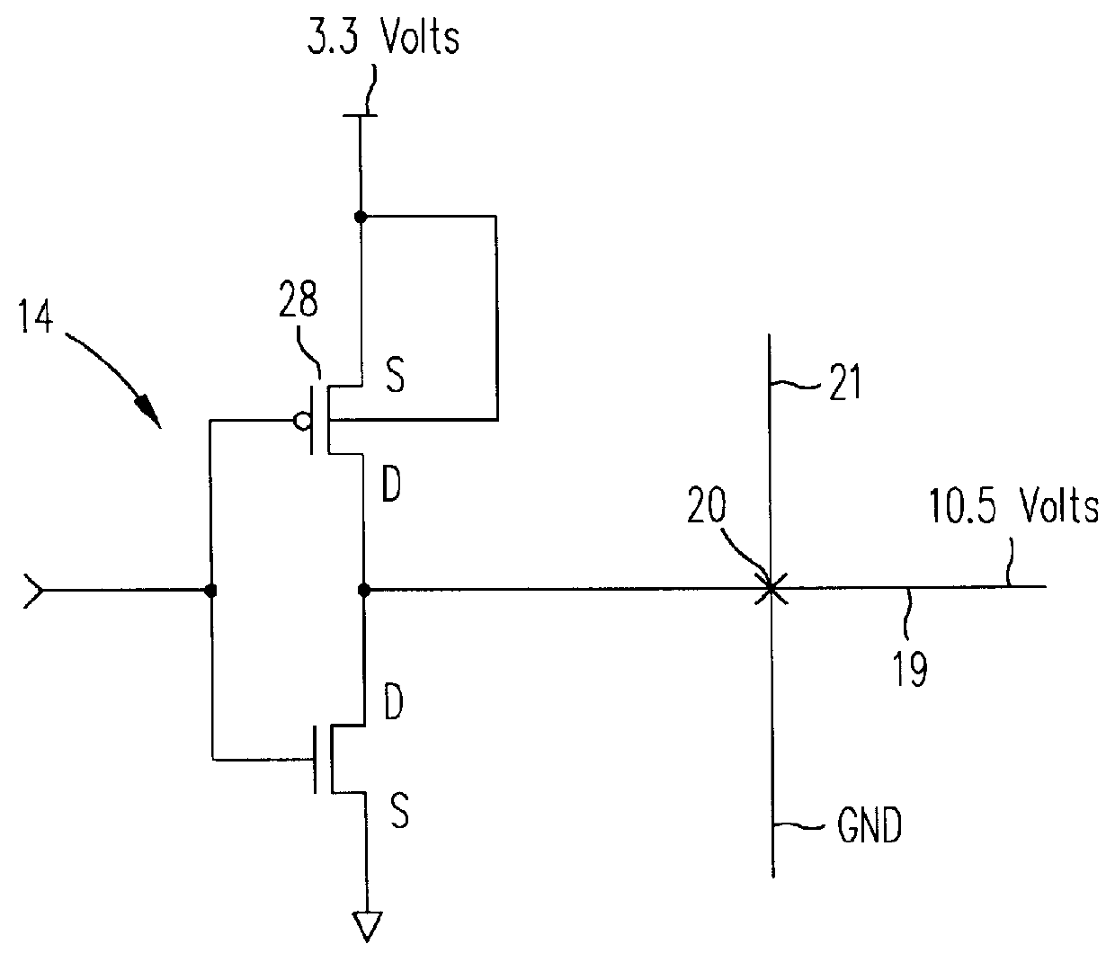
The first supply voltage power input terminal (VCC1) and the first ground terminal (GND1) are both coupled to the same potential (such as both grounded or both coupled to supply voltage VCC) during antifuse programming. The programming control circuits 103, on the other hand, are powered via second supply voltage power input terminal (VCC2) during antifuse programming. Second ground terminal (GND2) is grounded during antifuse programming and during normal circuit operation.
example 3
Only one of the first supply voltage power input terminal (VCC1) and the first ground terminal (GND1) is floated during antifuse programming. If the first supply voltage power input terminal (VCC1) is floated, then the first ground terminal GND1 is grounded (for example, coupled to second ground terminal GND2). If the first ground terminal (GND1) is floated, then the first supply voltage power input terminal (VCC1) is coupled to supply voltage VCC (for example, 3.3 volts). The programming control circuits 103, on the other hand, are powered via second power supply voltage power input terminal (VCC2) during antifuse programming when the second ground terminal (GND2) is grounded.
example 4
The first supply voltage power input terminal (VCC1) and the first ground terminal (GND1) are both coupled during antifuse programming to the same potential that is greater than supply voltage VCC but is less than the programming voltage Vpp. The programming control circuits 103, on the other hand, are powered during antifuse programming via second power voltage supply input terminal (VCC2). Second ground terminal (GND2) is grounded during antifuse programming.
In example four, the field programmable gate array still requires output protection transistors but the internal disable signal is omitted and the two associated transistors in each of the many logic module input devices are also omitted. Removing the two transistors from each logic module input device results in considerable space savings because there are so very many logic module input devices on the field programmable gate array. In one embodiment, terminals VCC1 and GND1 are coupled to approximately 5.5 volts during antif...
PUM
 Abstract
Description
Claims
Application Information