High VSWR mismatch output stage

a high-voltage standing wave ratio and output stage technology, applied in single-ended push-pull amplifiers, modulation, transmission monitoring, etc., can solve problems such as transistor failure, amplifier driving high-voltage standing wave load may suffer serious degradation, and unwanted standing wav

Inactive Publication Date: 2000-10-24
MAXIM INTEGRATED PROD INC
View PDF7 Cites 32 Cited by
  • Summary
  • Abstract
  • Description
  • Claims
  • Application Information

AI Technical Summary

Problems solved by technology

In communication systems, failure to match impedances causes unwanted standing waves resulting from signal reflection at the load.
For reasons described below, an amplifier driving high VSWR load may suffer from serious degradation due to mismatched loads.
Exceeding the SOA can result i

Method used


Image

  • High VSWR mismatch output stage
  • High VSWR mismatch output stage
  • High VSWR mismatch output stage

Examples


Embodiment Construction

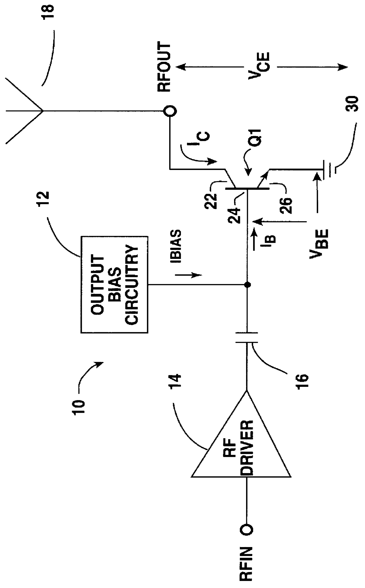
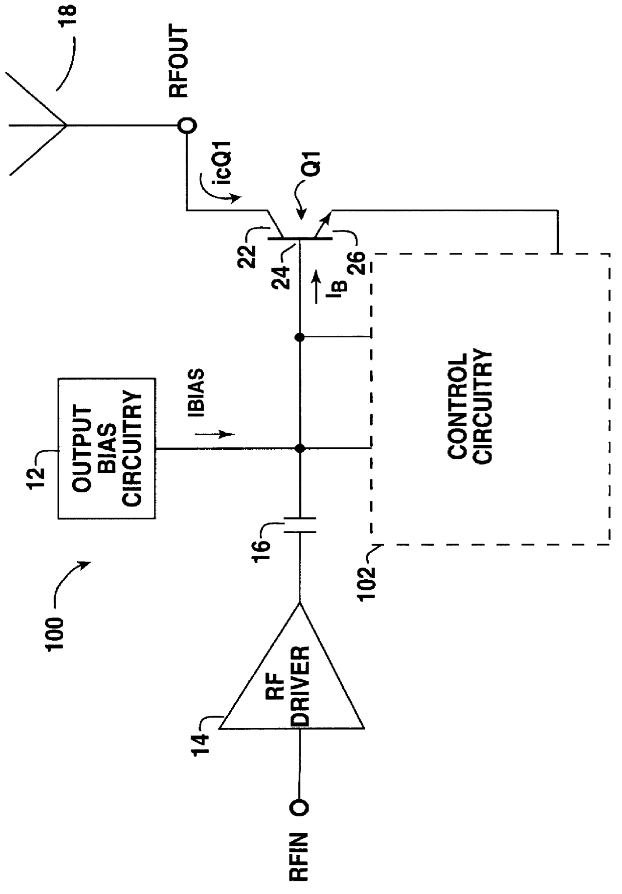
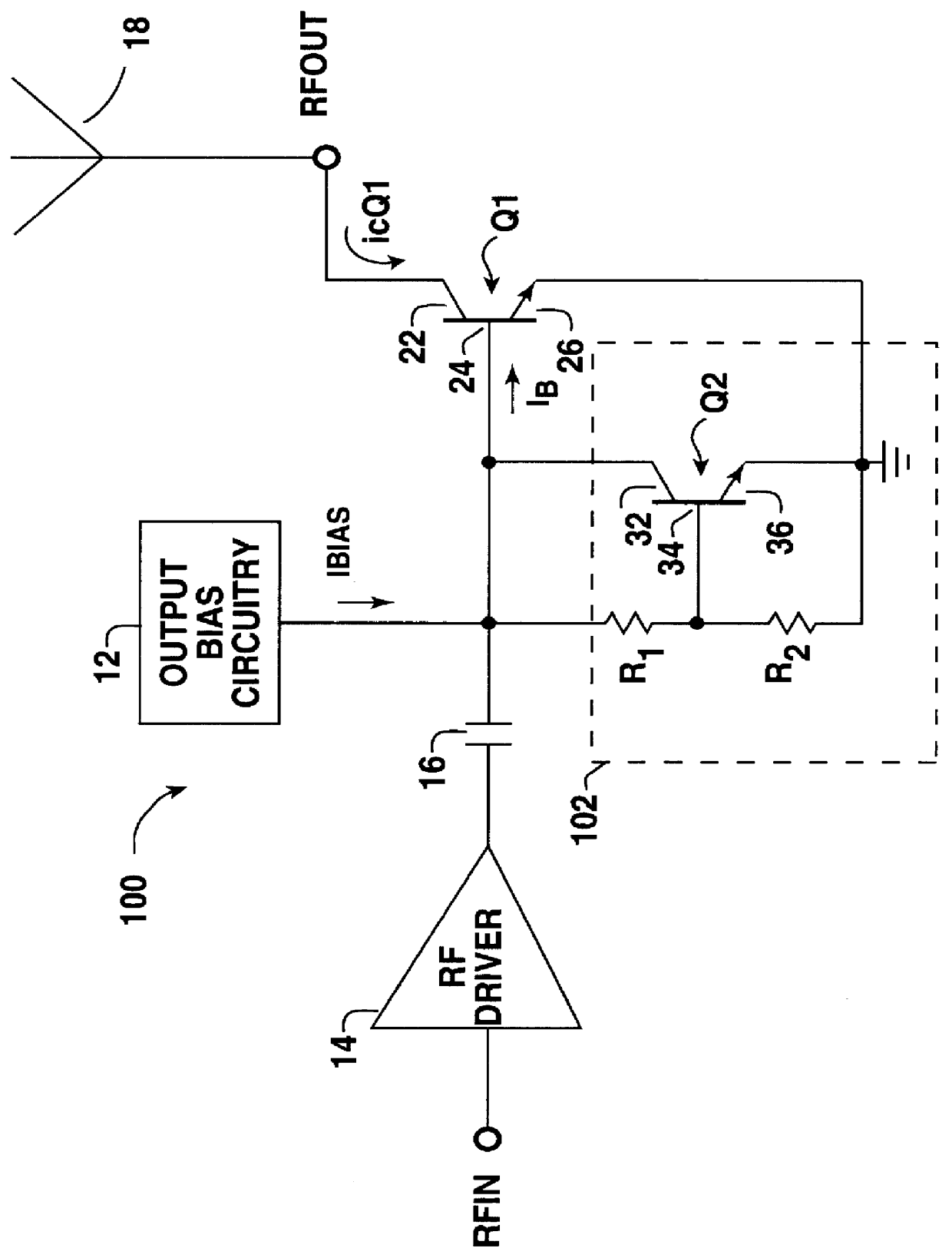
With reference to FIG. 2, a power amplifier 100 in accordance with one embodiment of the present invention will now be described. The power amplifier 100 includes a power npn transistor Q1, output bias circuitry 12, an RF driver 14, a capacitor 16, and control circuitry 102. The npn transistor Q1 has a collector 22 coupled to a terminal labeled RFOUT, a base 24, and an emitter 26 coupled to a common ground reference 30. The terminal labeled RFOUT may be coupled to an antenna 18.

The RF driver 14 amplifies an RFIN signal and then outputs the amplified signal to the capacitor 16. The capacitor 16 essentially serves to remove any DC component of the amplified output of the RF driver 14, leaving only the AC component to control the transistor Q1. The output bias circuitry 12 is coupled to the base 24 and injects a substantially constant current I.sub.bias into the base 24. The current I.sub.bias biases the transistor Q1 into an initial state such that, under "normal" operating conditions...


PUM


Abstract

The present invention teaches a variety of high VSWR mismatch output stages and methods for protecting output stages during high VSWR operation. To accomplish these goals, the present invention teaches absorbing reverse base current arising at the base of the power transistor of the output stage. In one embodiment, a variable impedance device such as a transistor is coupled to the base of the power transistor such that when the base-emitter voltage exceeds a predefined voltage, the variable impedance device goes into a low impedance mode and absorbs a portion of the base current. In another embodiment, feedback control circuitry is incorporated into the output stage bias circuitry in order to control the total base current.

Description

DESCRIPTION1. Technical FieldThe present invention is related to radio frequency (RF) power amplifiers. More specifically, the present invention teaches a variety of high voltage standing wave ratio (VSWR) mismatch output stages for use in RF power amplifiers.2. Background ArtFIG. 1 illustrates an RF power amplifier 10 of the prior art. The RF power amplifier 10 is well suited for applications such as cellular phones, cordless phones, two way pagers, wireless LANs, and AM and FM analog transmitters. As will be appreciated, depending upon the complexity and / or cost of the system, the RF power amplifier 10 may serve simply as a driver amplifier, or may be the complete power amplifier for the system.The power amplifier 10 includes a power npn transistor Q1, output bias circuitry 12, an RF driver 14, and a capacitor 16. The npn transistor Q1 has a collector 22 coupled to a terminal labeled RFOUT, a base 24, and an emitter 26 coupled to a common ground reference 30. The RF driver 14 ampl...

Claims


Application Information

Patent Timeline
IPC IPC(8): H03F3/189H03F1/30H03F3/19H02H7/20
CPCH03F1/302H03F3/19H03F1/52
Inventor KING, JOEL R.
Owner MAXIM INTEGRATED PROD INC
Why Eureka
Try Eureka