Multiple level cache memory with overlapped L1 and L2 memory access

a cache memory and memory access technology, applied in the field of computer systems, can solve the problems of performance penalty, unrealistic full access time of the second level cache,

Inactive Publication Date: 2000-10-24
IBM CORP
View PDF8 Cites 56 Cited by
  • Summary
  • Abstract
  • Description
  • Claims
  • Application Information

AI Technical Summary

Problems solved by technology

This mode of operation gives the highest performance, of course, but it is not realistic.
As

Method used


Image

  • Multiple level cache memory with overlapped L1 and L2 memory access
  • Multiple level cache memory with overlapped L1 and L2 memory access
  • Multiple level cache memory with overlapped L1 and L2 memory access

Examples


Embodiment Construction

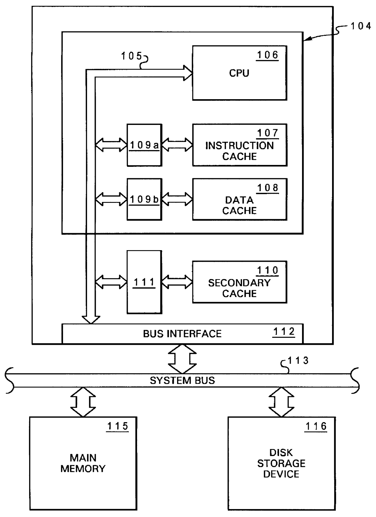
With reference now to the figures, and in particular with reference to FIG. 2, there is illustrated a block diagram of a data processing system in which a cache memory may be incorporated according to one embodiment of the invention. In FIG. 2, only a single processor 104 is shown; however, the features of the present invention are also useful in a multi-processor system. Processor 104, having a CPU 106 which may be of a superscalar RISC type, is constructed as a single-chip device comprising on-chip instruction cache 107 and data cache 108. Both caches 107, 108 are connected to CPU 106 by separate paths within a local bus structure. Instruction cache 107 is connected to local bus 105 via cache controller 109a, while data cache 108 is connected to local bus 105 via cache controller 109b. A secondary cache 110 is also connected to local bus 105 via cache controller 111. Secondary cache 110 is much larger than either instruction cache 107 or data cache 108, and access to secondary cac...


PUM


Abstract

A method of providing simultaneous, or overlapped, access to multiple cache levels to reduce the latency penalty for a higher level cache miss. A request for a value (data or instruction) is issued by the processor, and is forwarded to the lower level of the cache before determining whether a cache miss of the value has occurred at the higher level of the cache. In the embodiment wherein the lower level is an L2 cache, the L2 cache may supply the value directly to the processor. Address decoders are operated in parallel at the higher level of the cache to satisfy a plurality of simultaneous memory requests. One of the addresses (selected by priority logic based on hit/miss information from the higher level of the cache) is gated by a multiplexer to a plurality of memory array word line drivers of the lower level of the cache. Some bits in the address which do not require virtual-to-real translation can be immediately decoded.

Description

1. Field of the InventionThe present invention generally relates to computer systems, and more particularly to an improved method of accessing a cache memory of a processing unit, wherein the cache has a multi-level architecture, to reduce memory access latency.2. Description of Related ArtA typical structure for a conventional computer system includes one or more processing units connected to a system memory device (random access memory or RAM) and to various peripheral, or input / output (I / O), devices such as a display monitor, a keyboard, a graphical pointer (mouse), and a permanent storage device (hard disk). The system memory device is used by a processing unit in carrying out program instructions, and stores those instructions as well as data values fed to or generated by the programs. A processing unit communicates with the peripheral devices by various means, including a generalized interconnect or bus, or direct memory-access channels. A computer system may have many additio...

Claims


Application Information

Patent Timeline
IPC IPC(8): G06F12/08
CPCG06F12/0897G06F12/0884G06F12/08
Inventor DHONG, SANG HOOHOFSTEE, HARM PETERMELTZER, DAVIDSILBERMAN, JOEL ABRAHAM
Owner IBM CORP
Why Eureka
Try Eureka