Pixel drive circuit, image capture device, and camera system

a pixel drive and image capture technology, applied in the field of pixel drives, can solve the problems of large amount of control, temporary voltage drop in the pixel drive circuit, and malfunction of the circuit, and achieve the effect of not lowering the image quality of the captured imag

Inactive Publication Date: 2009-04-02
SONY CORP
View PDF4 Cites 30 Cited by
  • Summary
  • Abstract
  • Description
  • Claims
  • Application Information

AI Technical Summary

Benefits of technology

[0029]According to embodiments of the present invention, there may be provided a pixel drive circuit in which an image quality of a captured image is not lowered

Problems solved by technology

Due to an increased number of pixels and lowered power consumption in recent years, there occurs a problem of triggering a temporary voltage drop in the pixel drive circuit or other circuits during the global shutter.
This problem occurs because when the number of pixels is further increased, the pixel circuits driv

Method used


Image

  • Pixel drive circuit, image capture device, and camera system
  • Pixel drive circuit, image capture device, and camera system
  • Pixel drive circuit, image capture device, and camera system

Examples


Embodiment Construction

[0044]With reference to drawings, embodiments of the present invention are described below.

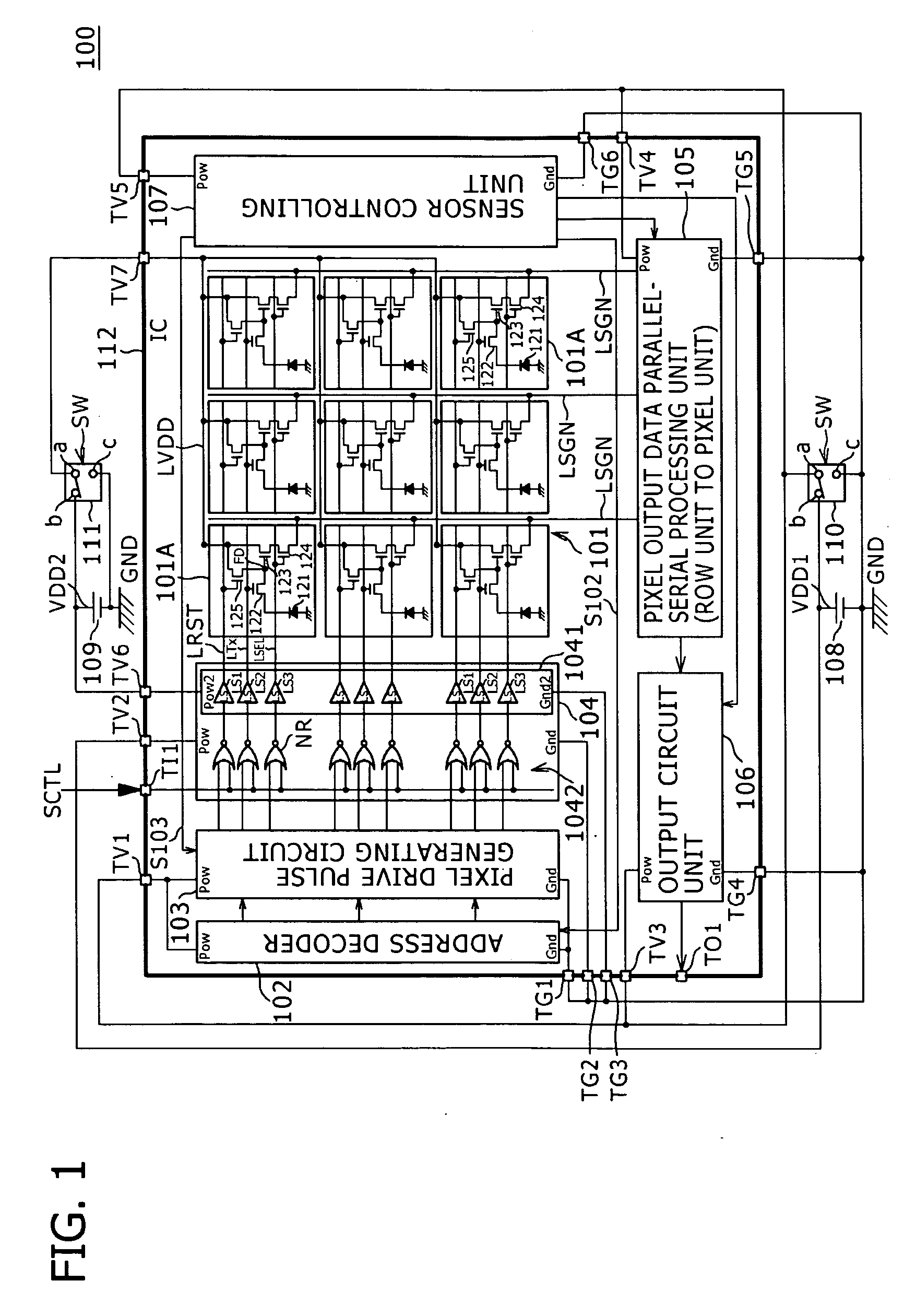
[0045]FIG. 1 is a diagram showing a configuration example of a CMOS image sensor according to an embodiment of the present invention.

[0046]A CMOS image sensor (image capture device) 100 illustrated in FIG. 1 includes a pixel array unit 101, an address decoder 102, a pixel drive pulse generating circuit 103, a pixel drive unit 104, a pixel output data parallel-serial processing unit 105, an output circuit unit 106, a sensor controlling unit 107, external power supplies (batteries) 108 and 109, and switches 110 and 111.

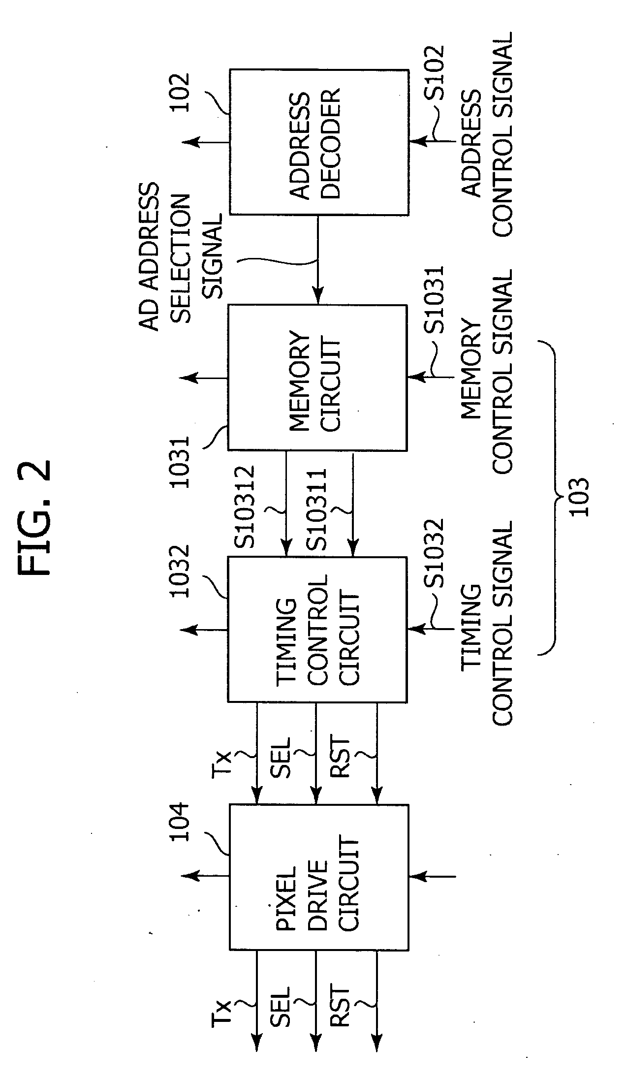
[0047]Noted, the address decoder 102, the pixel drive pulse generating circuit 103, and the pixel drive unit 104 correspond to a pixel drive circuit of the present invention and the pixel output data parallel-serial processing unit 105 corresponds to a reading unit of an embodiment of the present invention, respectively.

[0048]Out of these constituent elements, the pixel array unit...


PUM


Abstract

A pixel drive circuit includes a plurality of pixel circuits each including a photoelectric converting unit for converting an incident light into an electric charge and accumulating the converted electric charge, the plurality of pixel circuits being arranged in a matrix shape, an address decoder for selecting the pixel circuits to be controlled which are arranged on an identical line, a storage circuit for storing operation information to be executed by the pixel circuits selected by the address decoder, and a control circuit for controlling an operation of the pixel circuits selected by the address decoder in accordance with a storage state of the storage circuit. The control circuit controls a charge discharging operation of discharging an electric charge remaining in the photoelectric converting unit of each of the pixel circuits. The storage circuit holds the storage state until the charge discharging operation is completed.

Description

BACKGROUND OF THE INVENTION[0001]1. Field of the Invention[0002]The present invention relates to a pixel drive circuit of a CMOS (Complementary Metal Oxide Semiconductor) type, for example, an image capture device, and a camera system.[0003]2. Description of the Related Art[0004]A CMOS image sensor (image capture device) has a plurality of advantages as follows: a partial reading which is difficult in a CCD (Charge Coupled Device) is possible; the image sensor can be driven by a single power supply; and an analog circuit and a logical circuit using a CMOS process may be mounted together on an identical chip. Because of the advantages, the CMOS image sensor is widely used for a camera, et al.[0005]In such a CMOS image sensor, as shown in FIG. 12, a photodiode 11 as a photoelectric conversion element for converting an incident light into an electric charge is widely used. A pixel circuit 1 transfers the electric charges accumulated in the photodiode 11 via a transfer transistor 12 to ...

Claims


Application Information

Patent Timeline
IPC IPC(8): H04N5/228H04N5/335H04N5/357H04N5/369H04N5/374H04N5/376
CPCH04N3/1568H04N5/376H04N5/3597H04N25/626H04N25/74H04N25/745H04N25/76H04N25/75
Inventor FUJITA, NORITAKATAKAMIYA, KENICHIKOSEKI, KENUI, HIROKI
Owner SONY CORP
Why Eureka
Try Eureka