SWL ferroelectric memory and circuit for driving the same

a ferroelectric memory and circuit technology, applied in the direction of information storage, static storage, digital storage, etc., can solve the problems of unstable reference voltage, rapid degradation of reference cells, unstable reference voltage,

Inactive Publication Date: 2000-07-18
HYUNDAI ELECTRONICS IND CO LTD
View PDF13 Cites 29 Cited by
  • Summary
  • Abstract
  • Description
  • Claims
  • Application Information

AI Technical Summary

Problems solved by technology

However, in the background art 1T / 1C FRAM, in which the reference cell is operative more than the main memory cell, the reference cell degrades rapidly, providing an unstable reference voltage.
Further, the regulation of the reference voltage by using a voltage regulating circuit is also not stable due to influences from an external power characteristic and noise.
In spite of its merit that a stored data is kept when the power is off, the conventional FRAM has a complex layout because of their separated plate lines, and therefore, the manufacturing process is also complicated.
The integration in the conventional ferroelectric memory cell also cannot be improved without developing a new electric material or a new barrier material.
Another important factor causing a serious problem in the integration is that the area of a FRAM is larger than that of DRAM having the same capacity since a capacitor cannot be formed on a silicon substrate or on a surface of polysilicon because of lack of technique forming a ferroelectric layer on a surface of silicon.
Moreover, it is difficult to exactly control the operation of the memory device since the wordline and the plate line are separately controlled, and therefore, there is a difference between control signals according to the transmission path.
Further, particularly in the background art 1T / 1C FRAM, since one reference cell of a ferroelectric substance of which ferroelectric property is not fully assured is provided for a few hundreds of main memories for use in reading operation, requiring much more operation of the reference cell, the reference cell is involved in a rapid degradation of the ferroelectric property, causing instability of the reference voltage.

Method used


Image

  • SWL ferroelectric memory and circuit for driving the same
  • SWL ferroelectric memory and circuit for driving the same
  • SWL ferroelectric memory and circuit for driving the same

Examples


third embodiment

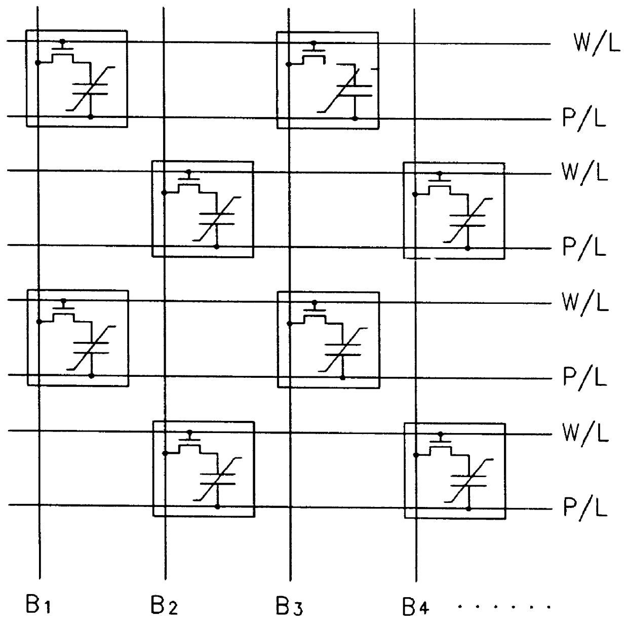
FIG. 10 illustrates a circuit of an SWL ferroelectric memory cell array in accordance with the present invention. The cell array includes a plurality of D first split wordlines SWL1.sub.-- n, SWL1.sub.-- n+1, SWL1.sub.-- n+2, SWL1.sub.-- n+3, etc., a plurality of second split wordlines SWL2.sub.-- n, SWL2.sub.-- n+1, SWL2.sub.-- n+2, SWL2.sub.-- n+3, etc., on one side of the split wordlines, a plurality of bitlines B.sub.-- n, B.sub.-- n+1, etc., and a plurality of bitbarlines BB.sub.-- n, BB.sub.-- n+1, etc, crossing the first, and second split wordlines, and the memory cells formed at intersections of the first and second split wordlines, and odd and even numbered bitlines, respectively, of the plurality of bitlines.

The memory cells can be formed of a folded bitline system in which the memory cell is provided, not at every crossing of the first and second split wordlines with the bitlines, but in view of a particular split wordline, one for every second bitline. Accordingly, the s...

first embodiment

The operation of the global control pulse generator of the present invention more or less differs depending on cell array systems, X, Z-address toggle, or Y-address toggle. The operation of the global control pulse generator is shown in FIG. 31, which is the first embodiment, in a case when the cell array system of FIG. 8 or 9 and the Y-address is toggled. Because the chip is enabled when the chip enable signal CSBpad signal applied externally is at "low", the chip will be brought into an enabled state when the CSBpad signal is turned from "high" to "low". Therefore, a disabled interval at a "high" state is required for conducting a new read or write. As shown in FIG. 31, one complete cycle of operation is divided from t1 interval to t15 interval, for convenience of explanation of signal behaviors.

First, it is assumed that the CSBpad signal is enabled at "low" from a starting point of the t1 interval to an end point of the t4 interval and disabled at "high" from a starting point of ...

second embodiment

The operation of the global control pulse generator is shown in FIG. 32, which is the second embodiment, in a case when the cell array system of FIG. 8 or 9 and the X, Z-address are toggled. One complete cycle of operation is divided from t1 interval to t21 interval, and both X, Z-addresses are transited at starting points of t7 and t14 intervals. Because the operation of the global control pulse generator in a case of the X, Z-address toggle is also similar to the operation of the operation of the global control pulse generator in the case of the Y-address toggle, portions of which operations are different will be explained.

While Y-ATD signal is transited to "high" at a time point when a Y-address is transited in FIG. 31, as it is assumed in the second embodiment of the present invention that both X, Z-addresses are transited at starting points of t7 and t14 intervals, X, Z-ATD signals are held at "high" in t7 interval and t14 interval and at "low" in rest of the intervals. When th...


PUM


Abstract

A split wordline ferroelectric memory does not utilize plate lines and a circuit for driving the same is disclosed. The memory including unit cell arrays and each array has a plurality of split wordlines (SWLs) arranged in a first direction at fixed intervals, and a plurality of bitlines arranged in a second direction vertical to each of the SWLs at fixed intervals. A ferroelectric unit memory cell is arranged in each pair of adjacent two SWLs and adjacent two bitlines. The circuit includes a post X-decoder for receiving and decoding X and Z-addresses for controlling a cell array block operative, a global control pulse generator for providing a control pulse required for data write or read in response to a CSBpad signal received externally, a local control pulse generator for receiving the control pulse from the global control pulse generator and providing a control signal required for data write and read, an SWL cell array block for storage of data, an SWL driver for driving the SWL cell array block in response to control signals from the post X-decoder and the local control pulse generator, a Y-address decoder for decoding a Y-address signal received externally, a column controller for controlling columns in response to the control signal from the local control pulse generator and a decoded signal from the Y-address decoder, and a sense amplifier and I / O controller for sensing / recording a data from / to the SWL cell array block.

Description

BACKGROUND OF THE INVENTION1. Field of the InventionThe present invention relates to a non-volatile ferroelectric memory, and more particularly, to a circuit for driving a split wordline (SWL) ferroelectric memory.2. Background of the Related ArtA ferroelectric random access memory (FRAM) has a data processing speed as fast as a DRAM and conserves data even after the power is turned off. The FRAM includes capacitors similar to the DRAM, but the capacitors have a ferroelectric substance for utilizing the characteristic of a high residual polarization of the ferroelectric substance in which data is not lost even after eliminating an electric field applied thereto.FIG. 1A illustrates a general hysteresis loop of a ferroelectric substance, and FIG. 1B illustrates a construction of a unit capacitor in a background art ferroelectric memory. As shown in the hysteresis loop in FIG. 1A, a polarization induced by an electric field does not vanish, but remains at a certain portion ("d" or "a" ...

Claims


Application Information

Patent Timeline
Patent Type & Authority Patents(United States)
IPC IPC(8): G11C11/22
CPCG11C11/22
Inventor KANG, HEE BOK
Owner HYUNDAI ELECTRONICS IND CO LTD
Why Eureka
Try Eureka