Flash/dynamic random access memory field programmable gate array

a dynamic random access and memory field technology, applied in static storage, digital storage, instruments, etc., can solve problems such as charge decay

Inactive Publication Date: 2007-03-06
ACTEL CORP
View PDF10 Cites 31 Cited by
  • Summary
  • Abstract
  • Description
  • Claims
  • Application Information

AI Technical Summary

Problems solved by technology

A standard MOS transistor is able to store a charge, but the charge decays due to the inability of gate capacitance to maintain the charge.

Method used


Image

  • Flash/dynamic random access memory field programmable gate array
  • Flash/dynamic random access memory field programmable gate array
  • Flash/dynamic random access memory field programmable gate array

Examples


Embodiment Construction

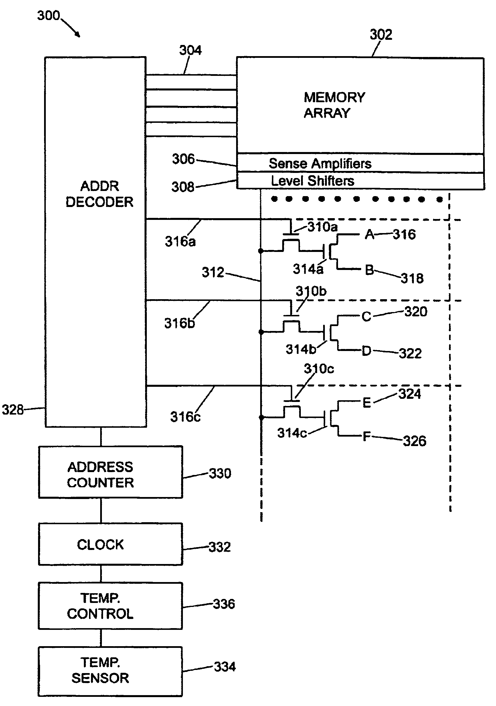
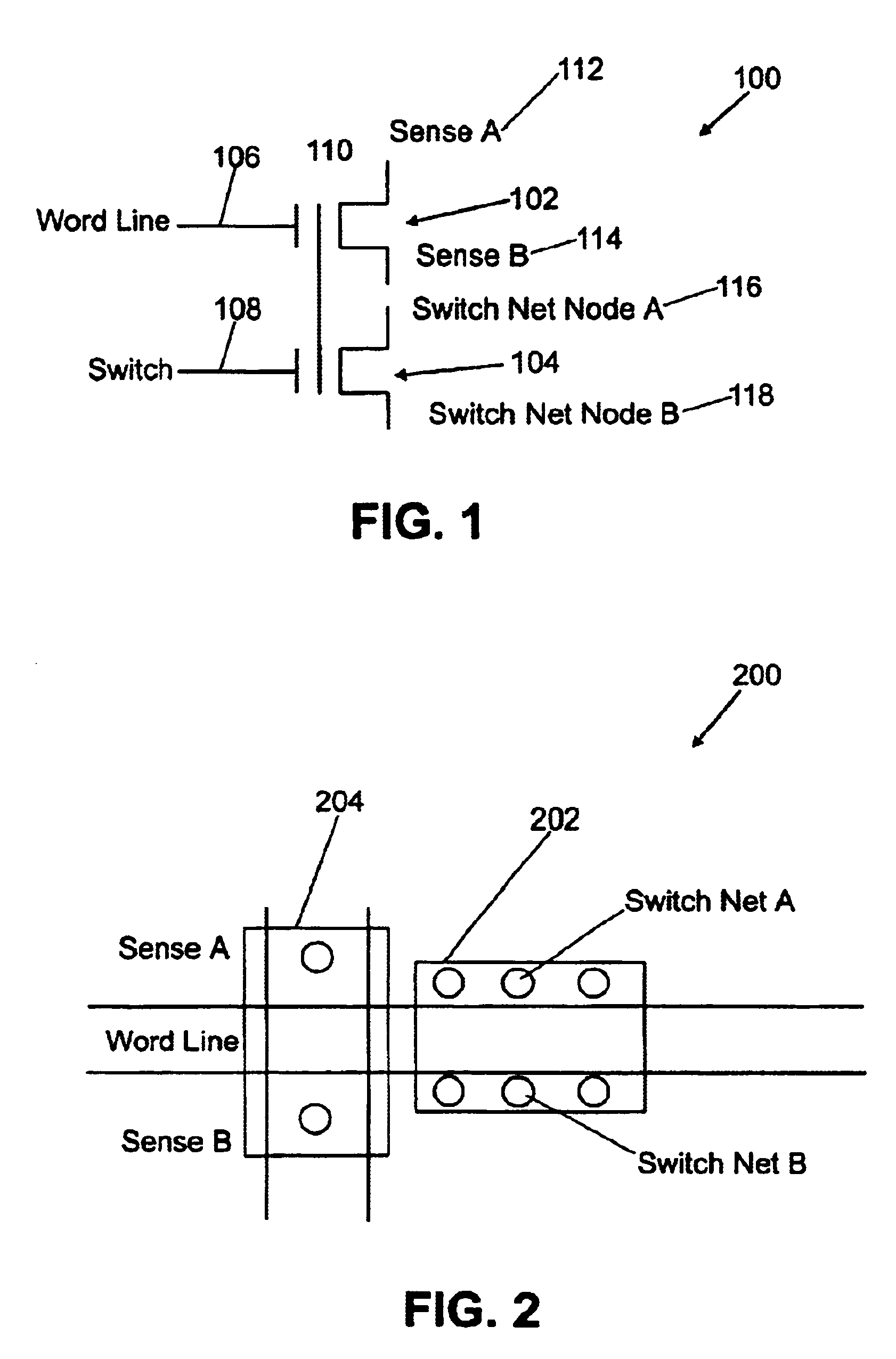
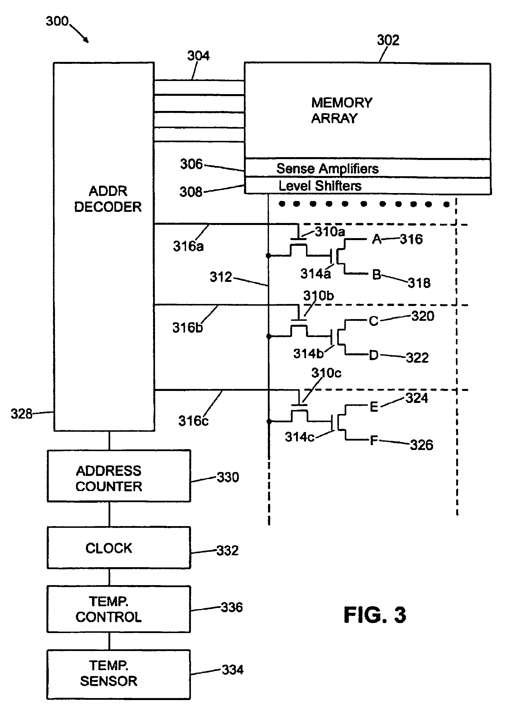
[0021]Those of ordinary skill in the art will realize that the following description of the present invention is illustrative only and not in any way limiting. Other embodiments of the invention will readily suggest themselves to such skilled persons.

[0022]In this disclosure, various circuits and logical functions are described. It is to be understood that designations such as “1” and or “0” in these descriptions are arbitrary logical designations. In a first implementation of the invention, “1” may correspond to a voltage high, while “0” corresponds to a voltage low or ground, while in a second implementation, “0” may correspond to a voltage high, while “1” corresponds to a voltage low or ground. Likewise, where signals are described, a “signal” as used in this disclosure may represent the application, or pulling “high” of a voltage to a node in a circuit where there was low or zero voltage before, or it may represent the termination, or the bringing “low” of a voltage at the node,...


PUM


Abstract

A method for providing a circuit for selectively interconnecting N pairs of nodes in an integrated circuit device comprising: providing a memory array having a plurality of wordlines and a plurality of bitlines; providing a plurality of dynamic random access memory wordlines; providing a separate switch for each pair of nodes in the integrated circuit, each switch associated with a unique combination of one of the plurality of bitlines and one of the plurality of dynamic random access memory wordlines, each switch including a refresh transistor and a switching transistor; and providing an address decoder having at least N distinct states for supplying signals to the plurality of wordlines and the plurality of dynamic random access memory wordlines.

Description

CROSS-REFERENCE TO RELATED APPLICATIONS[0001]This application is a continuation of U.S. patent application Ser. No. 11 / 113,286, filed Apr. 21, 2005 now U.S. Pat. No. 7,120,079, which is a continuation of U.S. patent application Ser. No. 10 / 623,111, filed Jul. 17, 2003, now issued as U.S. Pat. No. 6,891,769 issue date May 10, 2005, all of which are hereby incorporated by reference as if set forth herein.BACKGROUND[0002]1. Field of the Invention[0003]The present invention relates to memory cells in an integrated circuit. More specifically, the invention relates to using a standard transistor as a flash / dynamic random access memory (DRAM) in order to reduce the size of a gate oxide for a memory cell in an integrated circuit.[0004]2. Background[0005]FPGA integrated circuits are known in the art. Typically, an FPGA has an array of logic elements and wiring interconnections with many thousands of programmable interconnect cells so that the FPGA can be configured by the user into an integr...

Claims


Application Information

Patent Timeline
Patent Type & Authority Patents(United States)
IPC IPC(8): G11C7/00G11C8/00
CPCG11C7/04G11C7/1051G11C7/1057G11C11/404G11C11/406G11C16/3431G11C11/40626G11C11/4093G11C14/0018G11C11/40615G11C14/00G11C16/0441
Inventor MCCOLLUM, JOHNBELLIPPADY, VIDYABAKKER, GREGORY
Owner ACTEL CORP
Why Eureka
Try Eureka