Electron generation using a fluorescent element and image forming using such electron generation

a fluorescent element and electron generation technology, applied in the field of electron generation using fluorescent elements and image forming using such electron generation, can solve the problems of disturbance of display image around the support member, inability to fully correct, and change of color still occur,

Inactive Publication Date: 2000-10-31
CANON KK
View PDF10 Cites 10 Cited by
  • Summary
  • Abstract
  • Description
  • Claims
  • Application Information

AI Technical Summary

Problems solved by technology

However, in such flat type CRT's, disturbance of display image occurs around the support members.
The considerable main cause is electric charge-up of the support members which may influence the trajectories of electrons.
However, the disturbance of display image cannot be fully corrected by merely providing the conductivity to the support members, and the shift of light-emission position, luminance degradation, change of color still occur around the support members.
However, if the conductive connection member between the wiring electrodes and the spacer are thick, a slope of electric potential is generated around these members.
This causes shifting of the trajectories of electrons emitted from the electron-emitting devices.
A large difference between the conductive connection member's resistance value and the wiring electrodes' resistance values may cause disturbance of the electric field, however, a large difference between the spacer resistance value and the resistance values of other portions effects the electron trajectories around the wiring electrodes and the conductive connection member, at an ignorable level.

Method used


Image

  • Electron generation using a fluorescent element and image forming using such electron generation
  • Electron generation using a fluorescent element and image forming using such electron generation
  • Electron generation using a fluorescent element and image forming using such electron generation

Examples


first embodiment

Accordingly, in the following the present invention, an image display device using a multi electron source having the surface-conduction emission type electron-emitting devices formed using a fine-particle film, is used as a preferable example of the image forming apparatus of the present invention.

Note that in the following embodiments, the regularly arranged wiring electrodes partially connected to the support members are referred to as the "row-direction wiring electrodes". However, this name is made for the purpose of convenience of explanation, and it may also be replaced with the column-direction wiring electrodes, without causing any problem from the point of the present invention.

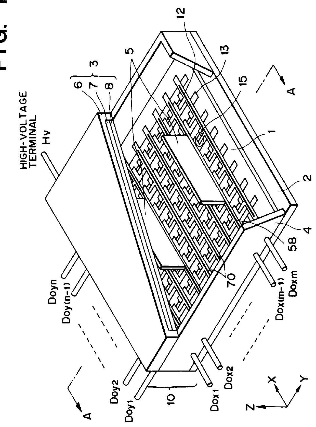
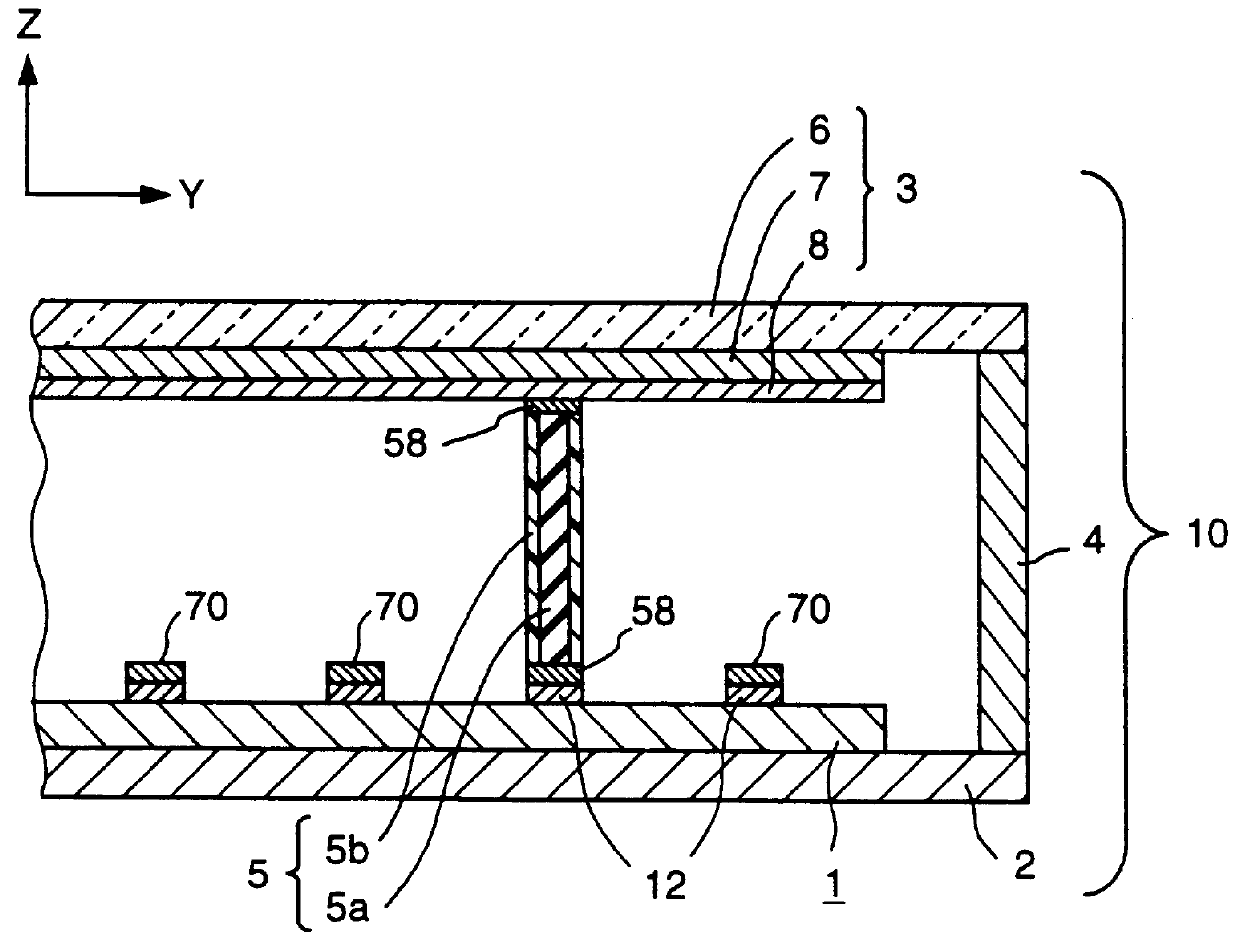
FIG. 1 is a partially-cutaway perspective view showing the structure of the image forming apparatus, and FIG. 2, a cross-sectional view of a significant part of the image forming apparatus in FIG. 1 cut along the line A-A'.

In FIGS. 1 and 2, the electron source 1 where the plurality of surface-conduc...

second embodiment

The second embodiment also realizes color-image display without disturbance of electron trajectories and with excellent color reproducibility.

In the present embodiment, upon forming the conductive connection member 58, regarding the row-direction wiring electrode 12 where the spacer 5 is provided, the conductive connection member 58 is formed between the spacer 5 and the electrode 12; and regarding the row-direction wiring electrode 12 where the spacer 5 is not provided, the conductive member 70 having the same shape of the conductive connection member 58 is formed on the electrode 12.

This reduces the amount of conductive connection material to be applied between the row-direction wiring electrode 12 and the spacer 5, thus enables mass production.

The present invention can be applied to any of cold cathode electron-emitting devices other than surface-conduction emission type electron-emitting devices. For example, an electron-emitting device having a pair of electrodes opposing to ea...

fourth embodiment

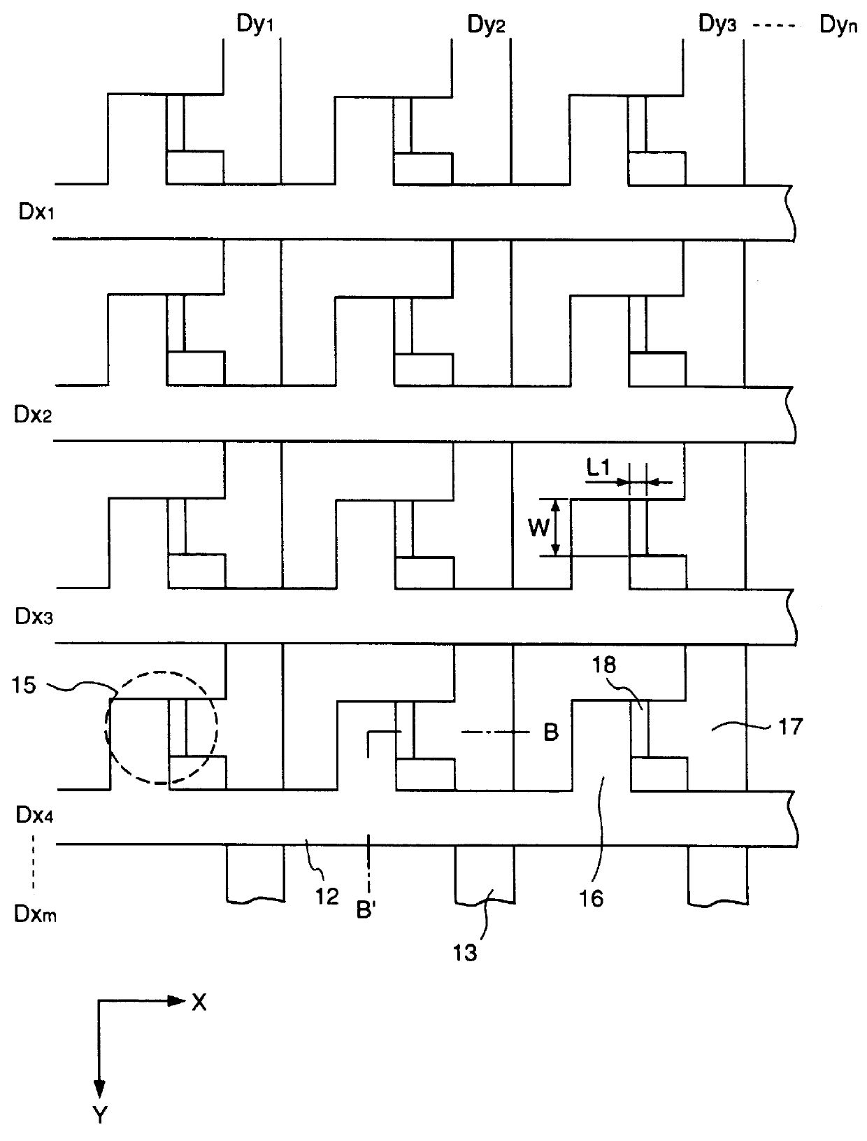
Next, the present invention will be described with reference to FIG. 26. In the manufacturing process according to this embodiment, the above-described printing step is divided into several steps to form a concave portion on the wiring electrodes for formation of conductive connection members.

Step e: Ag electrodes as the row-direction wiring electrodes 12 are formed by screen-printing, on the device electrodes 16 and 17. The screen-printing is performed twice, i.e., printing operations (a) and (b), using different screen masks at respective printing operations. The formed wiring-electrodes 12 have a concave portion 57 for application of the conductive connection member 58 having a thickness of 20 .mu.m.

The step e having the two printing operations will be described in detail with reference to FIG. 30. In FIG. 30, reference numeral 100 denotes electron-emitting portions; 11, the insulating substrate; 121 to 122, row-direction wiring electrodes; and 57, a concave portion for forming t...


PUM


Abstract

An image forming apparatus using an electron source which has matrix-wired electron-emitting devices connected with wiring electrodes of conductive material, and a fluorescent member as an image forming member with an accelerating electrode on its inner surface side, opposite to the electron-emitting devices. The wiring electrodes include a wiring electrode where a semiconductive support member (spacer) is provided via a conductive connection member and a wiring electrode where the semiconductive support member is not provided. The height of the upper surface of the conductive connection member on which the semiconductive support member is provided and that of the upper surface of the wiring electrode where the semiconductive support member is not provided are the same, to prevent shift of electron-beam trajectories around the semiconductive support member, due to disturbance of electric-field distribution.

Description

This invention relates to an electron-beam generating apparatus comprising a support member (spacer) and an image forming apparatus such as a display device, to which the electron-beam generating apparatus is applied to and, more particularly to an electron-beam generating apparatus comprising a large number of electron-emitting devices and an image forming apparatus using the electron-beam generating apparatus.[Description of Related Art]Generally, an image forming apparatus has an outer casing maintaining vacuum status, an electron source for emitting electrons and its driver, an image forming portion having a fluorescent member which emits light by collision of electrons or the like, an acceleration electrode for accelerating the electrons toward the image forming portion and its high-voltage power source. In an image forming apparatus having a flat outer casing such as a thin-type image display device, a support member (spacer) is employed to obtain atmospheric-pressure-proof st...

Claims


Application Information

Patent Timeline
Patent Type & Authority Patents(United States)
IPC IPC(8): H01J29/02H01J29/86H01J31/12
CPCB82Y10/00H01J29/028H01J29/864H01J31/127H01J2329/8655H01J2329/864H01J2329/8645
Inventor FUSHIMI, MASAHIROMITSUTAKE, HIDEAKISANOU, YOSHIHISA
Owner CANON KK
Why Eureka
Try Eureka