

Clock distribution network with dual wire routing
a technology of distribution network and clock line, applied in the direction of generating/distributing signals, pulse generators, pulse techniques, etc., can solve the problems of large area of metal layer, large consumption of power, and moderate power consumption
- Summary
- Abstract
- Description
- Claims
- Application Information
AI Technical Summary
Benefits of technology
Problems solved by technology
Method used
Image

Examples
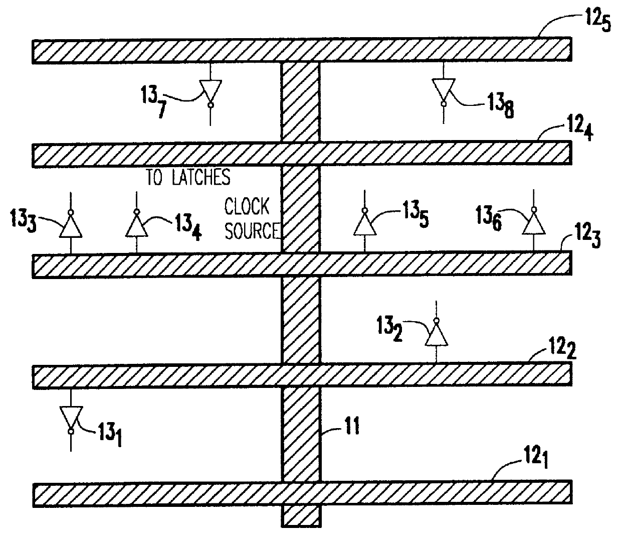
first embodiment
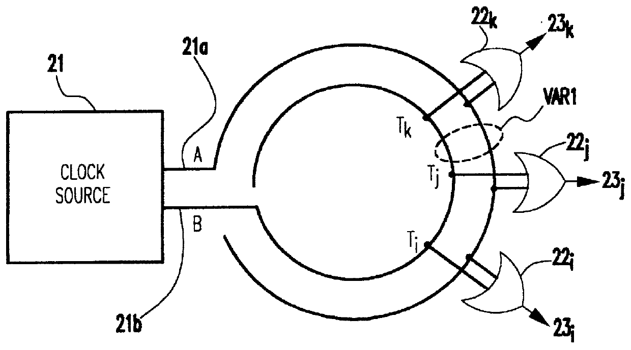
In the invention, shown in FIG. 2A, both wire A and wire B are driven directly by the clock source 21 by terminals 21a and 21b, respectively. The FIG. 2A embodiment is referenced hereinafter as the symmetrically driven embodiment.
second embodiment
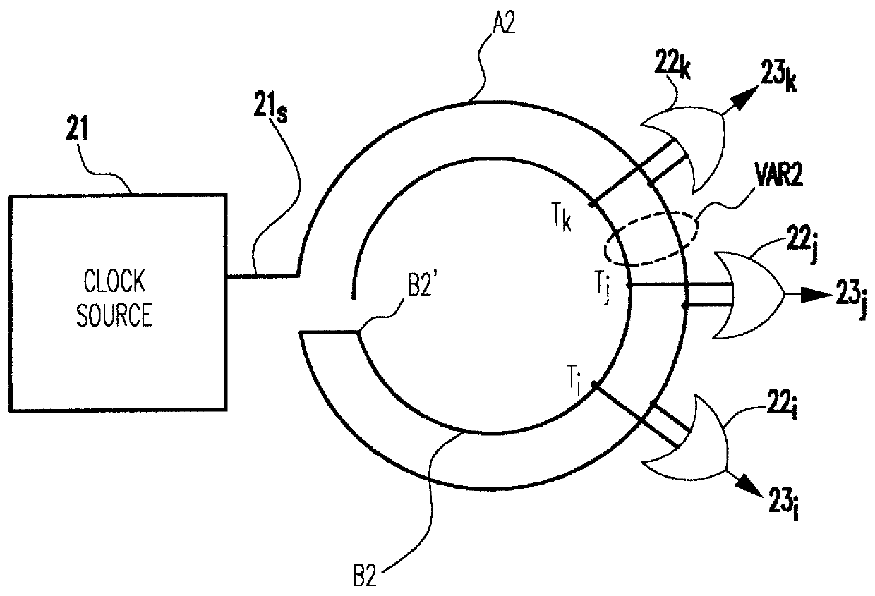
In the invention, shown in FIG. 2B, a first wire portion A2 is connected directly to the terminal 21s of clock source 21, while the end of wire portion A2 distal from the clock source 21 is connected to a second wire portion B2 be at B2'. The FIG. 2B embodiment is referenced hereinafter as the singly driven embodiment.
For both the FIGS. 2A and 2B example embodiments the length of each of wires A and B. and each of the wire portions A2 and B2, is L.
For the symmetrically driven embodiment of FIG. 2A, the clock signals from the clock source 21 appear simultaneously at terminals 21a and 21b which are connected respectively to wires A and B. The paths from the clock source terminals 21a and 21b, through wires A and B, to a tapping point T.sub.i are .rho.1=AT.sub.i and .rho.2=BT.sub.i, respectively. The corresponding path lengths are L1 and L2. The average path length to each of the tapping points Ti,Tj and Tk is (L1+L2), which is equal to one half the length L, (the length of both wires ...
PUM
 Abstract
Description
Claims
Application Information