Method, apparatus and computer program product for simulating diffusion of impurities in a semiconductor

a technology of impurities and computer programs, applied in the field of computer simulation methods, can solve problems such as affecting the diffusion of impurities, generating a large number of point defects, and becoming amorphous

Inactive Publication Date: 2000-11-28
NEC ELECTRONICS CORP
View PDF4 Cites 7 Cited by
  • Summary
  • Abstract
  • Description
  • Claims
  • Application Information

AI Technical Summary

Problems solved by technology

On the other hand, the region where a large number of point-defects generate during the ion implanting process become amorphous because the crystal structure of the region deteriorates.
At the interface between the re-crystallized region and the non-amorphous region, point-defects such as interstitial silicon atoms and holes are absorbed, thereby affecting the diffusio...

Method used


Image

  • Method, apparatus and computer program product for simulating diffusion of impurities in a semiconductor
  • Method, apparatus and computer program product for simulating diffusion of impurities in a semiconductor
  • Method, apparatus and computer program product for simulating diffusion of impurities in a semiconductor

Examples


first embodiment

Next, with reference to the accompanying drawings, the present invention will be explained.

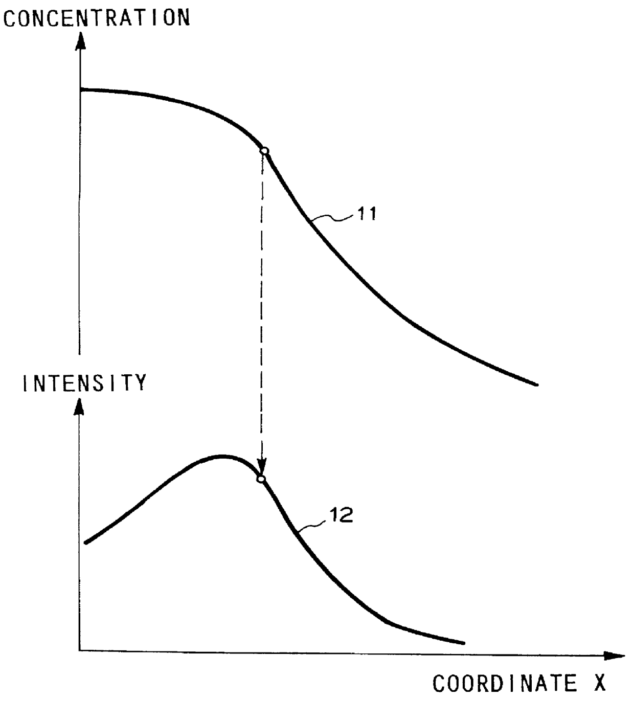
FIG. 1 is a graph for explaining the method of deriving the intensity of absorption of interstitial silicon (hereinafter referred to as suffix I), that is point-defects, in a diffusion simulating method according to the first embodiment of the present invention.

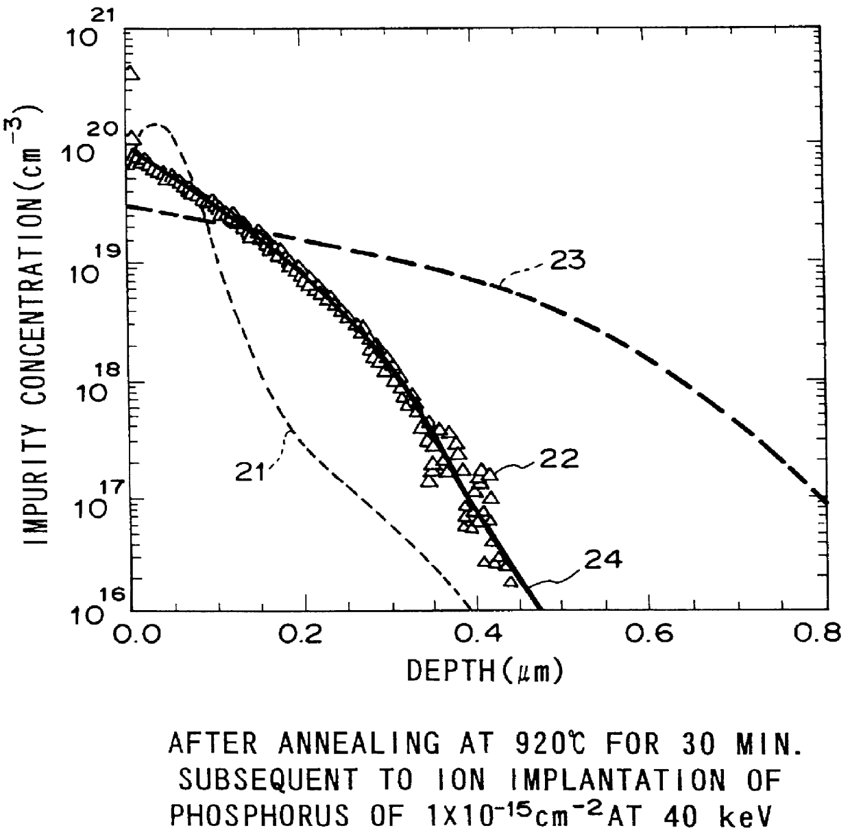
In this embodiment, the concentration C.sub.D (x) of initial point-defects (represented by curve 11 in FIG. 1) that generate in the ion implanting process is obtained with an ion implanting simulator. As a local function of the distribution of the concentration C.sub.D (x), the distribution of the intensity of absorption of interstitial silicon (represented by curve 12) is obtained. The distribution of the intensity K.sub.I (x, T) is obtained with the following equation.

K.sub.I (x, T)=f.sub.I (C.sub.D (x), T) (3),

where x represents an analytic coordinate vector that may be represented by two-dimensional or three-dimensional positional c...
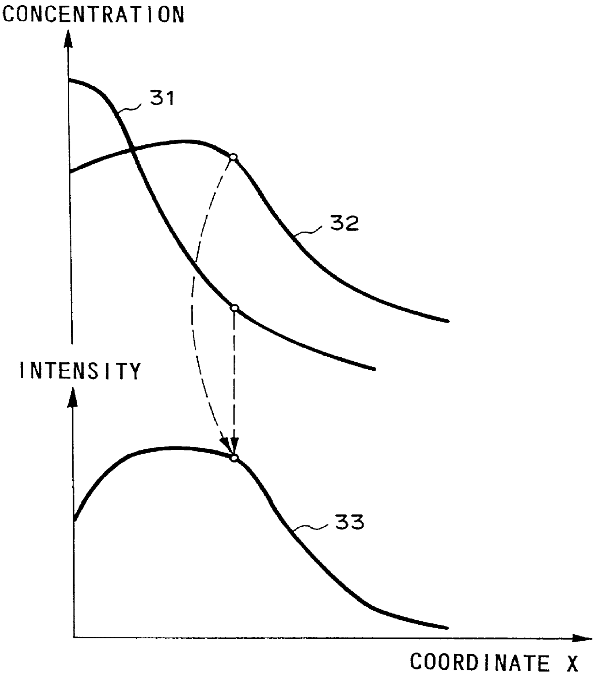
second embodiment

Next, the present invention will be explained.

The different point of this embodiment from the first embodiment is that the intensity of absorption of holes (hereinafter denoted by suffix V) is used instead of interstitial silicon atoms.

In the second embodiment, the distribution of the intensity of absorption of holes is obtained as a local function of the distribution of an initial concentration C.sub.D (x) of point-defects that generate in the ion implanting process. The local function is expressed as follows:

K.sub.V (x, T)=f.sub.V (C.sub.D (x), T) (7).

The term R.sub.V (x, t, T) representing the absorption of holes is expressed as follows:

R.sub.V (x, t, T)=K.sub.V (x, T)[C.sub.V (x, t)-C*.sub.V (T)](8),

where C.sub.V (x, t) represents the distribution of the concentration of holes; and C*.sub.V (T) represents the concentration of holes at the thermal equilibrium.

The term R.sub.V (x, t, T) is included in the diffusion equation.

third embodiment

Next, the present invention will be explained.

The different point of this embodiment from the former two embodiments is that the intensity of absorption of complex point-defects consisting of interstitial silicon atoms and impurity atoms or consisting of holes and impurity atoms is used.

In the third embodiment, the distribution of the intensity of complex point-defects (hereinafter denoted by a suffix X) is obtained as a local function of a distribution of an initial concentration C.sub.D (x) of point-defects that generate in the ion implanting process. This local function is expressed as follows:

K.sub.X (x, T)=f.sub.X (C.sub.D (x), T) (9).

The term R.sub.X (x, t, T) representing the absorption of complex points is expressed as follows:

R.sub.X (x, t, T)=K.sub.X (x, T)[C.sub.X (x, t)-C*.sub.X (T)](10),

where C.sub.X (x, t) represents the distribution of the concentration of complex point-defects; and C*.sub.X (T) represents the distribution of the concentration of the complex point-def...


PUM


Abstract

A distribution of the concentration of initial point-defects which generate in an ion implanting process is obtained with an ion implanting simulator. As a local function of the distribution, the distribution of the intensity of absorption of point-defects is obtained. A term of absorption of point-defects obtained from the distribution of the intensity is included in a diffusion equation. With the resultant diffusion equation, the diffusion simulation is performed. Thus the simulation using the diffusion equation may be extended to two or three dimension and cope with various ion implanting conditions.

Description

1. Field of the InventionThe present invention relates to a computer simulating method applied to a semiconductor fabrication process and, in particular, to an impurity diffusion simulating method which takes point-defects into account.2. Description of the Prior ArtUsing a computer, a process simulator calculates and predicts physical amounts and shapes of impurity profiles in a device fabricated by a semiconductor LSI fabrication process including an ion implanting process and an ion diffusing process. When the semiconductor LSI fabrication process is optimized for the maximum electric characteristics using the process simulator, the cost and time for designing LSI chips can be remarkably reduced as compared to the case that many experimental LSI chips are made and tested. In addition, since the process simulator calculates physical amounts of a semiconductor device, it can analyze actions of impurities in the semiconductor device. For details of the process simulator, refer to "T...

Claims


Application Information

Patent Timeline
IPC IPC(8): G06F17/50H01L21/265G06F19/00G06Q50/00G06Q50/04H01L21/00
CPCG06F17/5018G06F2217/80G06F30/23G06F2119/08H01L21/22
Inventor SAKAMOTO, HIRONORI
Owner NEC ELECTRONICS CORP
Why Eureka
Try Eureka