Method of making semiconductor device having double spacer

a semiconductor device and spacer technology, applied in the field of semiconductor devices, can solve the problems of reducing the threshold voltage, difficult to diffuse the dopant of the pocket implantation region, and semiconductor devices are generally subjected to a very rapid heat treatment at high temperatur

Inactive Publication Date: 2001-03-27
SAMSUNG ELECTRONICS CO LTD
View PDF4 Cites 50 Cited by
  • Summary
  • Abstract
  • Description
  • Claims
  • Application Information

AI Technical Summary

Problems solved by technology

In MOS devices, this leads to a decrease in the threshold voltage due to shortening of the channel.
One drawback to this prior art approach is that the semiconductor device is generally subjected to a very rapid heat treatment at high temperature for a short time in order

Method used


Image

  • Method of making semiconductor device having double spacer
  • Method of making semiconductor device having double spacer
  • Method of making semiconductor device having double spacer

Examples


Embodiment Construction

Reference will now be made in detail to the preferred embodiments of the present invention, examples of which are illustrated in the accompanying drawings.

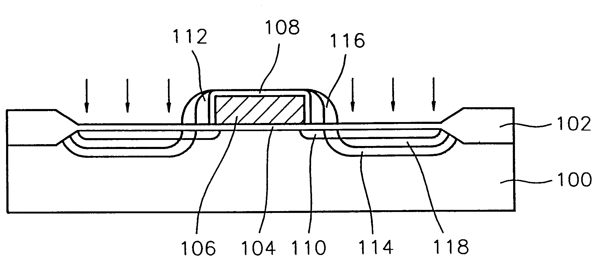
FIG. 4 is a schematic vertical cross section of a semiconductor device having a double spacer in accordance with the present invention. Referring to FIG. 4, the semiconductor device includes a device separating region 102 for defining the active region of devices formed in, for example, a p-type silicon substrate 100. A gate oxide layer 104 is formed over the surface of the active region in the substrate 100, a gate electrode 106 is formed over a selected region of the gate oxide layer 104, and a buffer oxide layer 108 is formed over the upper surface of the gate electrode 106. A first spacer 112 is formed on the sidewall of the buffer oxide layer 108, and a second spacer 116 is formed on the sidewall of the first spacer 112.

An LDD region 110 is formed as a first impurity region lightly doped with, for example, an n-type impurity ...


PUM


Abstract

A semiconductor device having a double spacer and a method of manufacturing the device are provided. The semiconductor device includes a first spacer formed on the sidewall of a gate electrode and a second spacer formed on the slanted sidewall of the first spacer. A first impurity region is formed doped with a first conductivity type impurity at a first concentration and formed at a small junction depth in the substrate to self-align at the edge of the gate electrode. A second impurity region doped with second conductivity type impurity at a second concentration is formed at a large junction depth in the substrate to self-align at the edge of the first spacer. A third impurity region doped with the first conductivity type impurity at a third concentration is formed at a medium junction depth in the second impurity region to self-align at the edge of the second spacer.

Description

1. Field of the InventionThe present invention relates to a semiconductor device and, more particularly, to a semiconductor device having a double spacer and a method of making the same to enhance the reliability of the semiconductor device.2. Discussion of Related ArtThe miniaturization of devices according to a scaling rule is used in a semiconductor device to achieve large-scale integration and high-speed operation. In MOS devices, this leads to a decrease in the threshold voltage due to shortening of the channel. Also, the effect of a depleted layer upon the channel in a source / drain region is reduced so as to attain a stable threshold voltage in the semiconductor device. To meet the requirements such as large-scale integration and high operational speed, semiconductor devices generally have a pocket implantation region or thin junction layer formed by a rapid heat treatment to increase the concentration of dopants in a localized region of the substrate.FIGS. 1-3 contain schemat...

Claims


Application Information

Patent Timeline
IPC IPC(8): H01L21/02H01L21/336H01L29/10H01L27/085H01L27/088H01L29/02H01L29/66H01L29/78H01L21/22
CPCH01L27/088H01L29/1083H01L29/6656H01L29/6659H01L29/665H01L29/7833Y10S257/90H01L21/22
Inventor KIM, HYUN-SIKSHIN, HEON-JONG
Owner SAMSUNG ELECTRONICS CO LTD
Why Eureka
Try Eureka