Adjustable feedback for CMOS latches

a technology of adjustable feedback and latches, applied in the field of digital logic systems, can solve the problems of excessive feedback during normal circuit operation, degrade performance and speed,

Inactive Publication Date: 2001-04-03
IBM CORP
View PDF4 Cites 30 Cited by
  • Summary
  • Abstract
  • Description
  • Claims
  • Application Information

AI Technical Summary

Problems solved by technology

Thus, there is always an engineering tradeoff between functionality and performance.
These conditions aggravate leakage and noise, thus requiring the designer to implement a greater amount of feedback to permit the circuit to function during

Method used


Image

  • Adjustable feedback for CMOS latches
  • Adjustable feedback for CMOS latches
  • Adjustable feedback for CMOS latches

Examples


Embodiment Construction

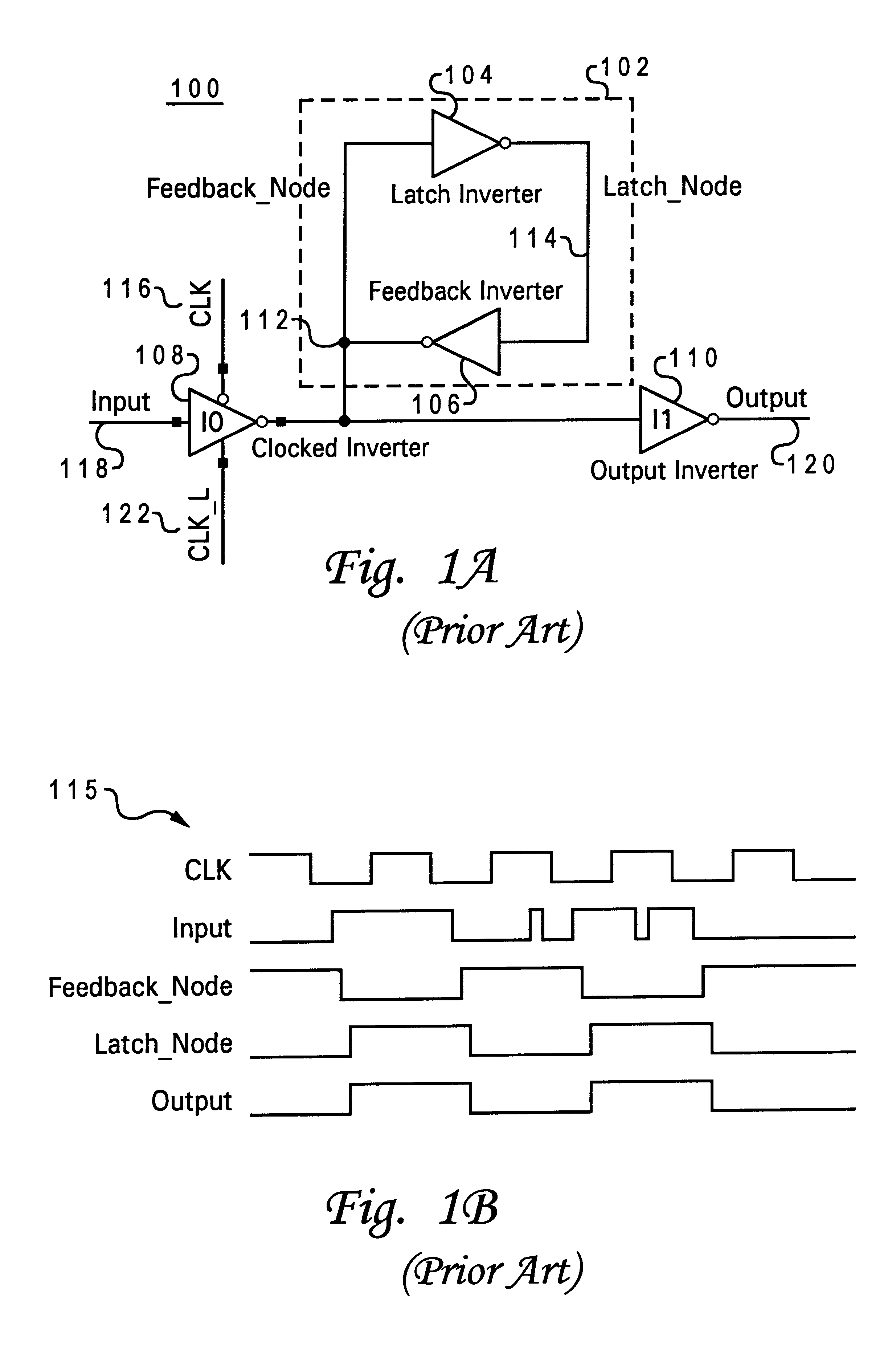
The system and method of the present invention provides integrated circuit designers control over the utilization of additional feedback for latches. Designers have conventionally had to design for the worst case circumstances which sacrifices performance in order to provide sufficient functionality during testing. The present invention allows designers to account for the variation in operating conditions that a CMOS latch may experience and adjust the feedback in the latch accordingly. Designers are thus provided the option to design for both performance in normal operating mode, and for functionality in high stress conditions such as burn-in and DVS testing.

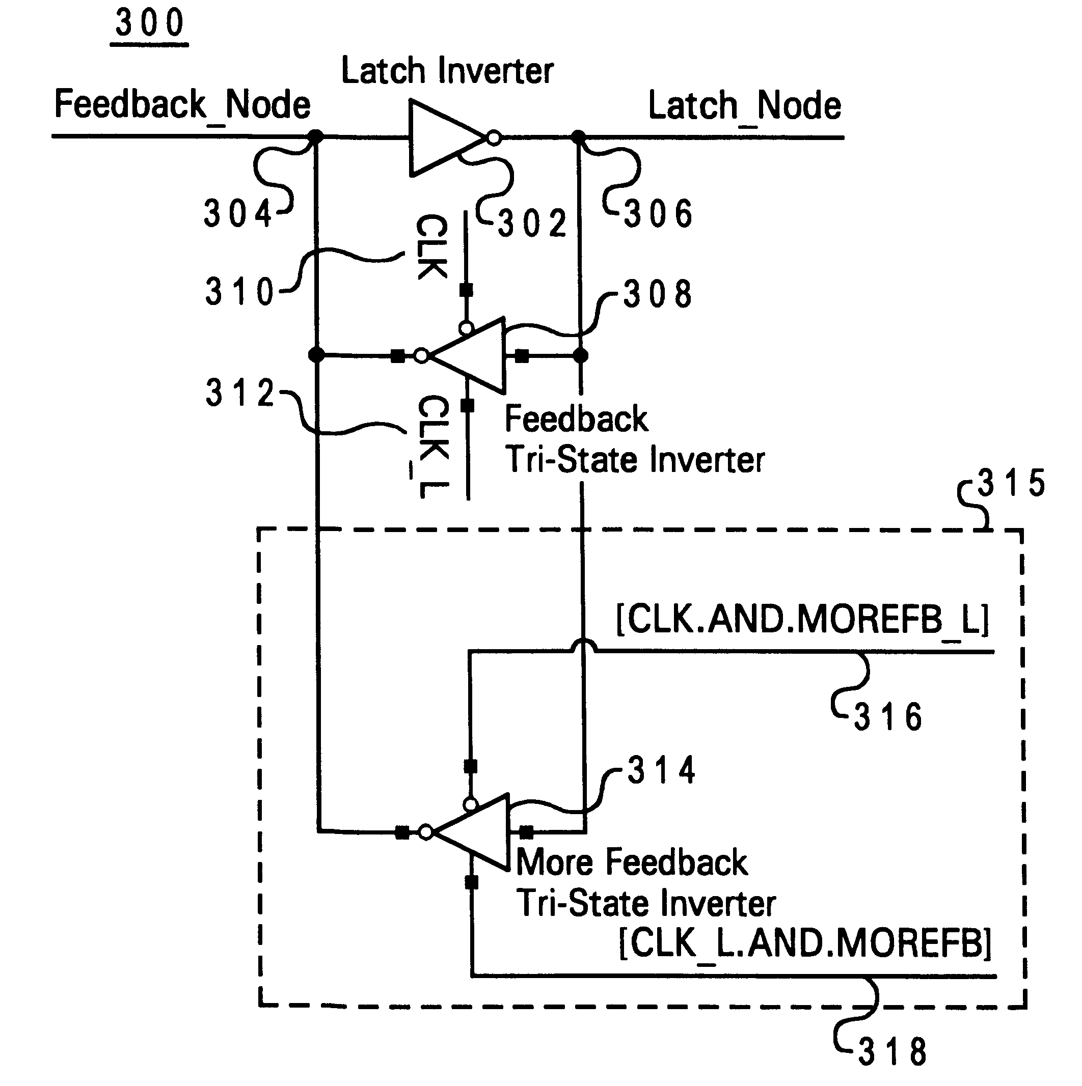
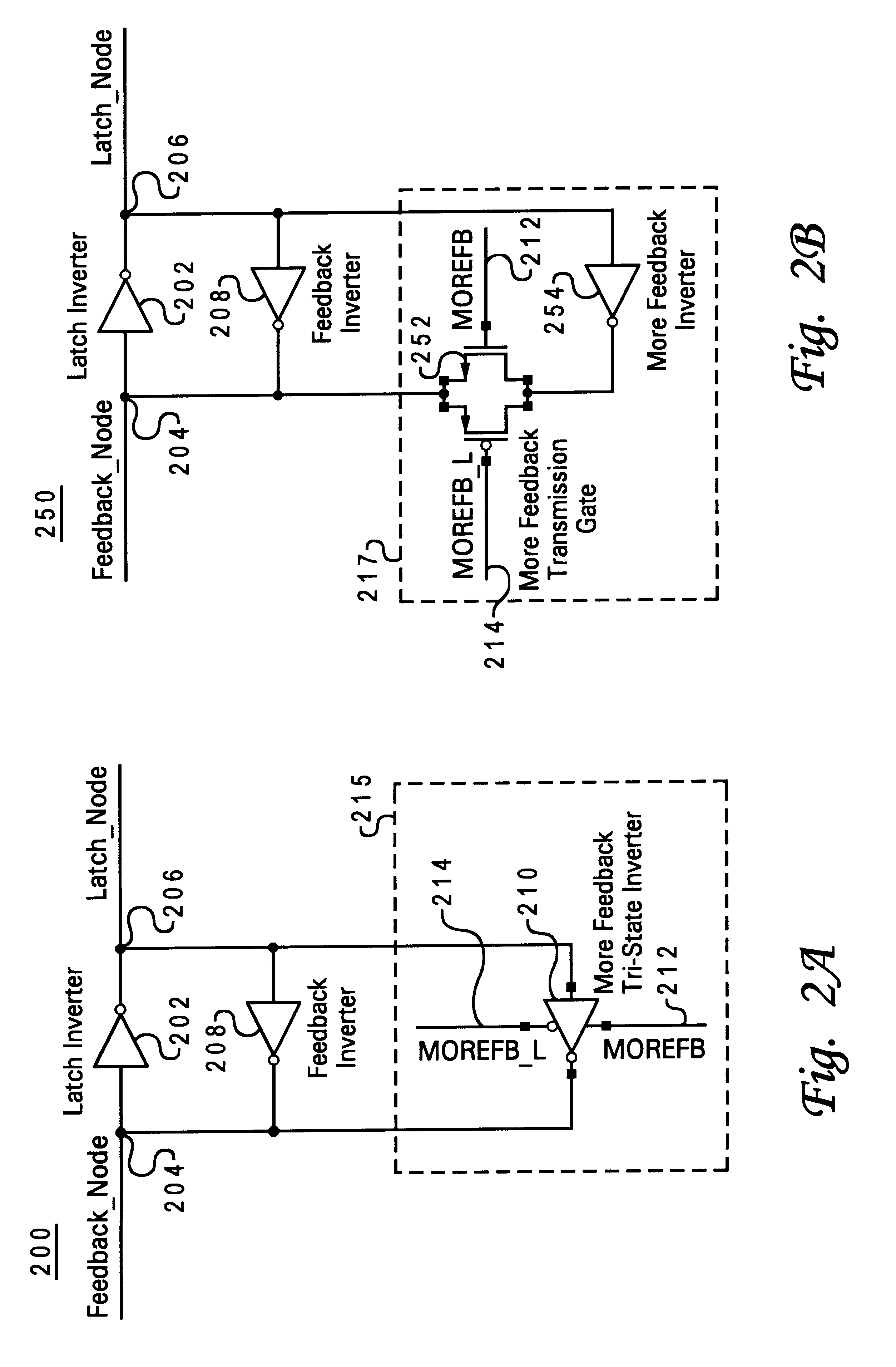
Turning now to the figures, and in particular to FIGS. 2A and 2B, there are depicted alternate embodiments of the improved latch circuit of the present invention. As illustrated in FIG. 2A, a Complementary Metal Oxide Semiconductor (CMOS) latch circuit 200 includes a latch inverter 202 and a feedback inverter 208. Although not ...


PUM


Abstract

An improved latch circuit having a dynamically adjustable internal feedback level. The improved latch circuit includes a latch inverter and a feedback inverter cross-coupled with the latch inverter. A controllable supplemental feedback inverter is connected in parallel with the feedback inverter to provide a controllable level of feedback to the latch inverter. An independently selectable control signal enables or disables the controllable feedback inverter in conformity with a need for more or less feedback, such that the internal feedback level may provide optimal functionality and performance of the latch circuit.

Description

The present invention relates in general to digital latches, and in particular to a method and system for altering the amount of feedback within a latch in conformity with actual operating requirements. Still more particularly, the present invention relates to a method and system which varies feedback within CMOS latch circuits to provide an optimal balance between functionality and performance of the circuit.DESCRIPTION OF THE RELATED ARTDigital logic systems may be generally categorized as either combinatorial or sequential. A combinatorial circuit consists of logic gates whose outputs at any time are determined directly from the values of the present inputs. A combinational circuit performs a specific information processing operation which can be specified logically by a set of Boolean expressions. Sequential circuits employ storage elements called flip-flops in addition to the logic gates. Their outputs are a function of the inputs and the state of the storage elements. The stat...

Claims


Application Information

Patent Timeline
IPC IPC(8): H03K3/037H03K3/00H03K3/012
CPCH03K3/012H03K3/037
Inventor UHLMANN, GREGORY JOHN
Owner IBM CORP
Why Eureka
Try Eureka