

Diode connected to a magnetic tunnel junction and self aligned with a metallic conductor and method for forming the same
a magnetic tunnel junction and diode technology, applied in the direction of semiconductor devices, electrical devices, nanotechnology, etc., can solve the problems of series resistance or low conductivity switch in series with the sense current path detracting from the signal, reducing the manufacturing yield of arrays of cells using tfd,
- Summary
- Abstract
- Description
- Claims
- Application Information
AI Technical Summary
Benefits of technology
Problems solved by technology
Method used
Image

Examples
first embodiment
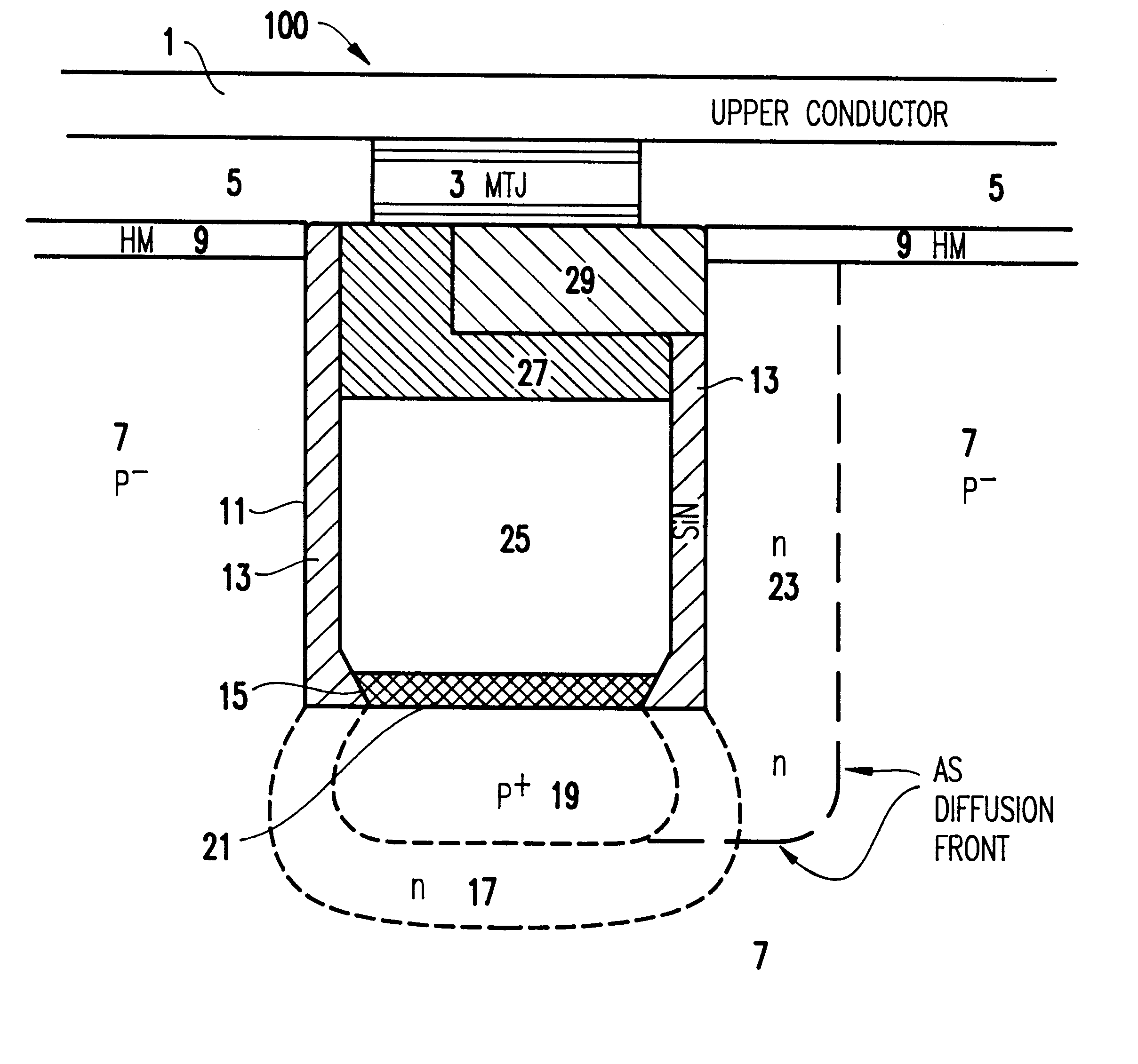
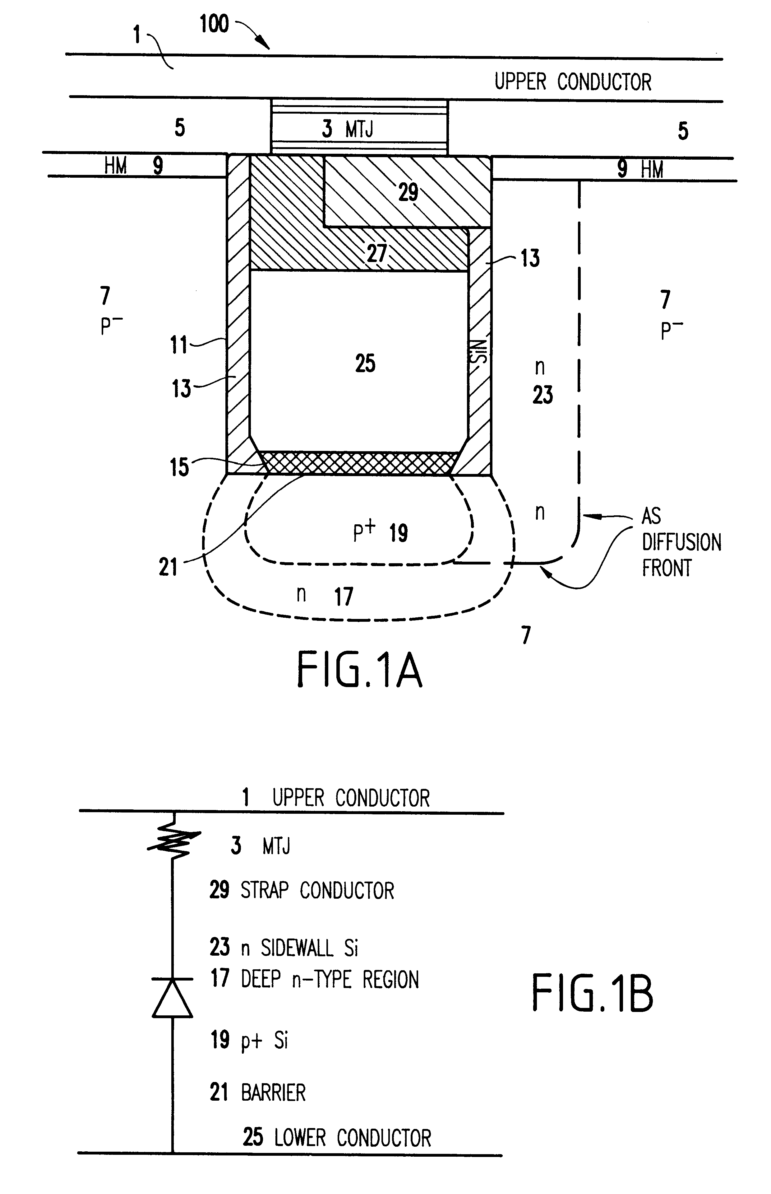
In FIG. 1A, a memory structure 100, preferably formed as an MRAM, is shown according to the present invention. Structure 100 includes an upper conductor (e.g., preferably formed of a thin film wire (TFW) such as copper which is a preferred metal material because of its low resistance) 1 is connected to each MTJ 3. Preferably, the upper conductor has a thickness of substantially within a range of about 0.2 .mu.m to about 0.6 .mu.m, and most preferably 0.4 .mu.m. Preferably, the MTJ has a thickness of substantially within a range of about 50 nm to about 300 nm, and most preferably 120 nm.
The space surrounding the MTJs and between the upper conductor 1 and the silicon substrate is filled with an interlayer dielectric 5, formed preferably of silicon dioxide.
Each MTJ is connected to, and fabricated upon, a strap conductor 29 (e.g., preferably formed of either metal or doped polysilicon) having a thickness in the range of about 0.02 to 0.1 .mu.m. The strap conductor 29 is planarized by ch...
second embodiment
A second embodiment according to the present invention is described below with reference to FIGS. 4A-4C.
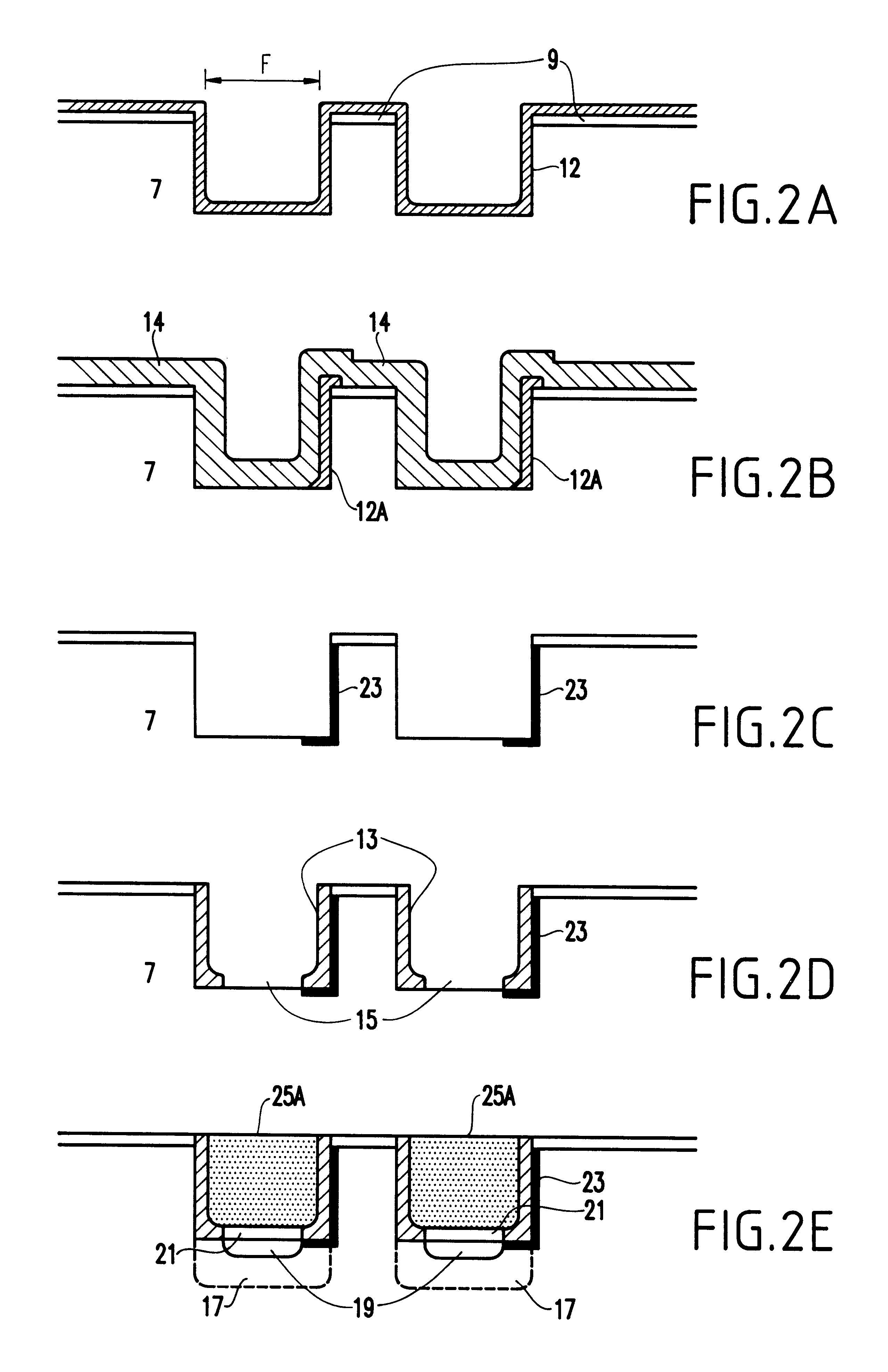
FIGS. 4A-4C show the second embodiment of the present invention wherein the diode is self-aligned to recessed regions denoted as V-grooves 414, and electrical connection to the bottom electrode of the diode (n region 415) is also self-aligned. An anisotropic wet etch or the like is used to make the recessed V-groove region in the silicon substrate. Materials and dimensions substantially similar to those described above can be employed, absent an indication to the contrary in the description below.
FIG. 4A is the plan view (top view) showing a bottom metal conductor (TFW) 425 drawn vertically, and three diodes formed at three recessed V-groove regions 414, respectively. In FIG. 4A, the three top metal conductors and the three MTJs are not shown, for clarity. It is noted that in FIG. 4A, the lines for V-grooves 414 are approximately 55.degree. diagonals, but generally do not meet in ...
third embodiment
FIGS. 5A-5C show the third embodiment of the present invention wherein the diode is self-aligned to recessed regions denoted as an etched recess in silicon 6 and the recess for the diode has a top portion with straight walls and a sloped portion below so the p region, which is on the sloped portion, is below the substrate surface.
FIG. 5A is a plan view showing a bottom metal conductor 525, drawn vertically, and two diodes 4 formed at two recessed regions 6. The two top metal conductors and the two MTJs are not shown, for clarity and ease of understanding. Similarly to FIG. 4A, STI 511 is formed outside rectangles 510, and is recessed at regions 511A.
FIG. 5B is a sectional view through plane A--A. Plane A--A becomes the center line of the top metal conductor in the completed memory array. The MTJ and the top metal conductor (not shown) in turn are formed above the structure shown. The V-groove is recessed to near the bottom of the n region 513, with substantially vertical walls in th...
PUM
 Abstract
Description
Claims
Application Information