System and method of optically inspecting manufactured devices

a manufactured device and optical inspection technology, applied in the direction of semiconductor/solid-state device testing/measurement, image enhancement, instruments, etc., can solve the problems of reducing the accuracy of optical inspection, and affecting the inspection accuracy of manufactured devices

Inactive Publication Date: 2001-06-12
RUDOLPH TECHNOLOGIES INC
View PDF4 Cites 48 Cited by
  • Summary
  • Abstract
  • Description
  • Claims
  • Application Information

AI Technical Summary

Problems solved by technology

First, when a component has the same color as the background, the component is effectively camouflaged relative to the PCB, making it difficult for the computer to determine where the edges of a component are placed and thereby provide the location of the component.
This reduces the accuracy of the optical inspection since a misplaced component may not be reported as a defect.
Alternatively, since the component may not be accurately traced, it may be reported as a defect even though it is correctly placed.
Furthermore, since existing optical inspection devices view the components from directly above, it is difficult to determine whether components are properly seated (vertically) even when they are in a proper location.
Finally, since each manufacturer may manufacture electrically

Method used


Image

  • System and method of optically inspecting manufactured devices
  • System and method of optically inspecting manufactured devices
  • System and method of optically inspecting manufactured devices

Examples


Embodiment Construction

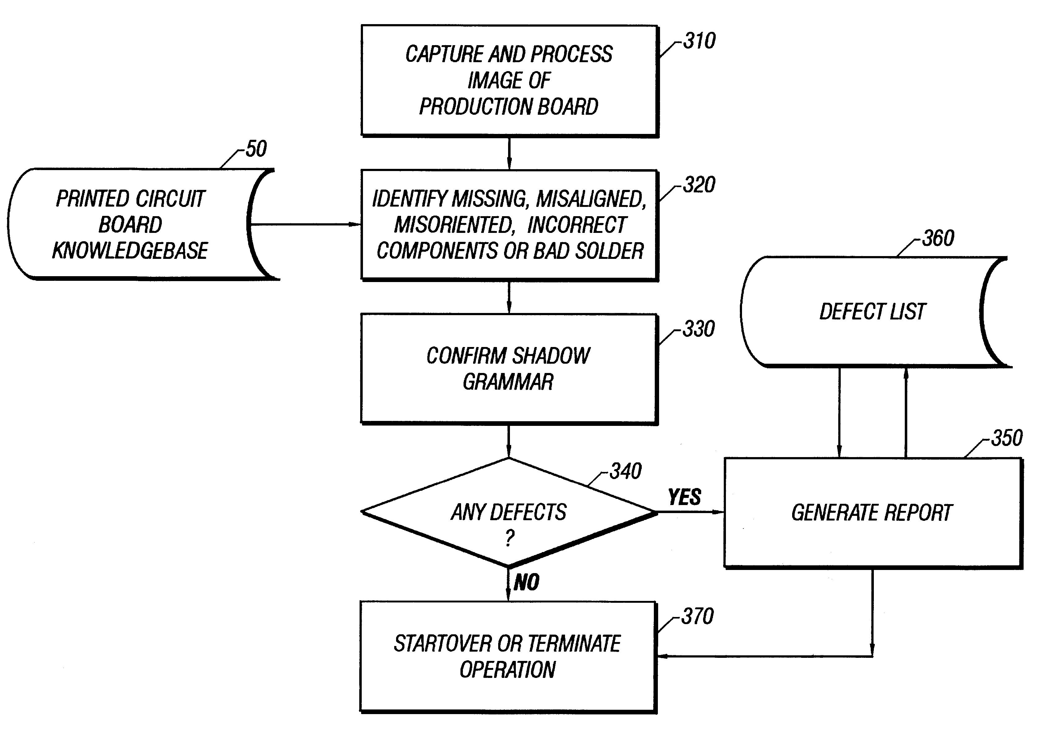
The present invention provides an apparatus, system and method of optically inspecting manufactured devices. In particular, the present invention optically inspects printed circuit boards (PCBs), reliably traces components having the same color as the component background, and detects components which are not properly seated by detecting and tracing component shadows. Because it detects component shadows, it provides defect detection even when component colors or PCB colors are changed. Thus, the present invention solves the problems associated with prior art optical inspection techniques by comparing production PCB gradients to defect-free PCB gradients.

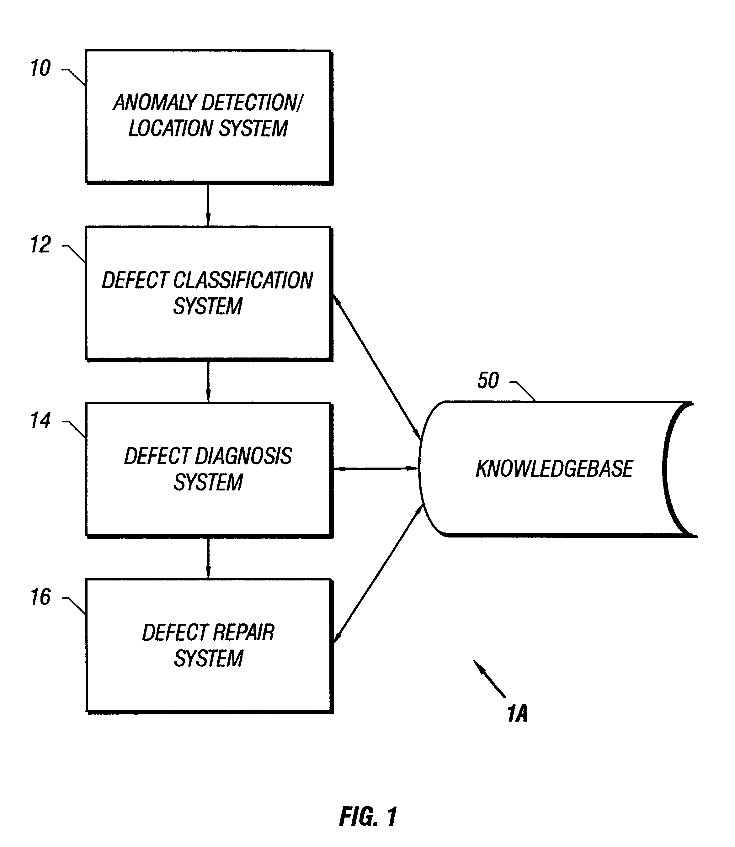
FIG. 1 is a block diagram illustrating the interrelations of sub-systems in an anomaly detection and correction system 1A. In the anomaly detection and correction system 1A there is an anomaly detection / location system 10, a defect classification system 12, a defect diagnosis system 14, a defect repair system 16, and a knowledge bas...


PUM


Abstract

An apparatus, system, and method of optically inspecting printed circuit boards (PCBs) for defects, that reliably determines the dimensions of components including those having the same color as the background, and which can detect components which are missing, misoriented, misaligned, or not properly seated. The apparatus uses a camera and a coherent primary light source mounted at an angle away from the vertical so as to produce sharply defined PCB component shadows on the top surface of the PCB. An image of the PCB is captured, the shadow edges are symbolically decomposed into primitives from which gradients are produced, and then compared to a previously captured gradient of a defect-free PCB. Differences in the two image gradients, if any, are used to identify missing, misaligned, misoriented, and improperly seated components, and to detect foreign objects and other PCB defects.

Description

1. Technical Field of the InventionThe present invention relates to the inspection of manufactured devices and, more specifically, to an apparatus, system, and method for optically inspecting Printed Circuit Boards (PCBs) for manufacturing defects such as missing components, misplaced components, skewed components, and foreign objects.2. Description of Related ArtPrinted Circuit Boards (PCBs) are typically constructed from a heat-resistant plastic base with selected channels cut therein for holding metallic conductors, and are usually covered with an insulative resin. PCBs simplify the construction of electronic devices such as computers, smoke detectors, stereos and other consumer electronics by providing a common support for, and the correct electrical connections between, electronic components such as resistors, capacitors, inductors, and digital devices. A manufacturer need only correctly place an appropriate electronic component on a PCB in a designated location and, because th...

Claims


Application Information

Patent Timeline
IPC IPC(8): G01N21/95G01N21/88G06T7/00H01L21/66
CPCG01N21/9501G06T7/0006H01L22/20G06T2207/10152G06T2207/30141H01L22/12H01L2924/0002H01L2924/014H01L2924/00
Inventor PATTIKONDA, RAMAKRISHNALIN, YOULINGHENNESSEY, KATHLEEN
Owner RUDOLPH TECHNOLOGIES INC
Why Eureka
Try Eureka