Cam array with minimum cell size

a technology of ram arrays and cell arrays, applied in the field of random access memory arrays, can solve the problems of difficult to read from non-volatile transistors mf1-mf2, difficult to read this array, and a relative large amount of time is required to read

Inactive Publication Date: 2001-07-03
AVAGO TECH INT SALES PTE LTD
View PDF8 Cites 57 Cited by
  • Summary
  • Abstract
  • Description
  • Claims
  • Application Information

AI Technical Summary

Problems solved by technology

Because each RAM read operation takes one clock cycle, a relatively large amount of time is required to read and compare a particular data value with all data values stored in a RAM array.
A problem with prior art CAM cell 100 is that the direct coupling of the gate of transistors MF1-MF2 to bit line BL and inverted bit line B...

Method used


Image

  • Cam array with minimum cell size
  • Cam array with minimum cell size
  • Cam array with minimum cell size

Examples


Embodiment Construction

4T Non-volatile CAM Cell

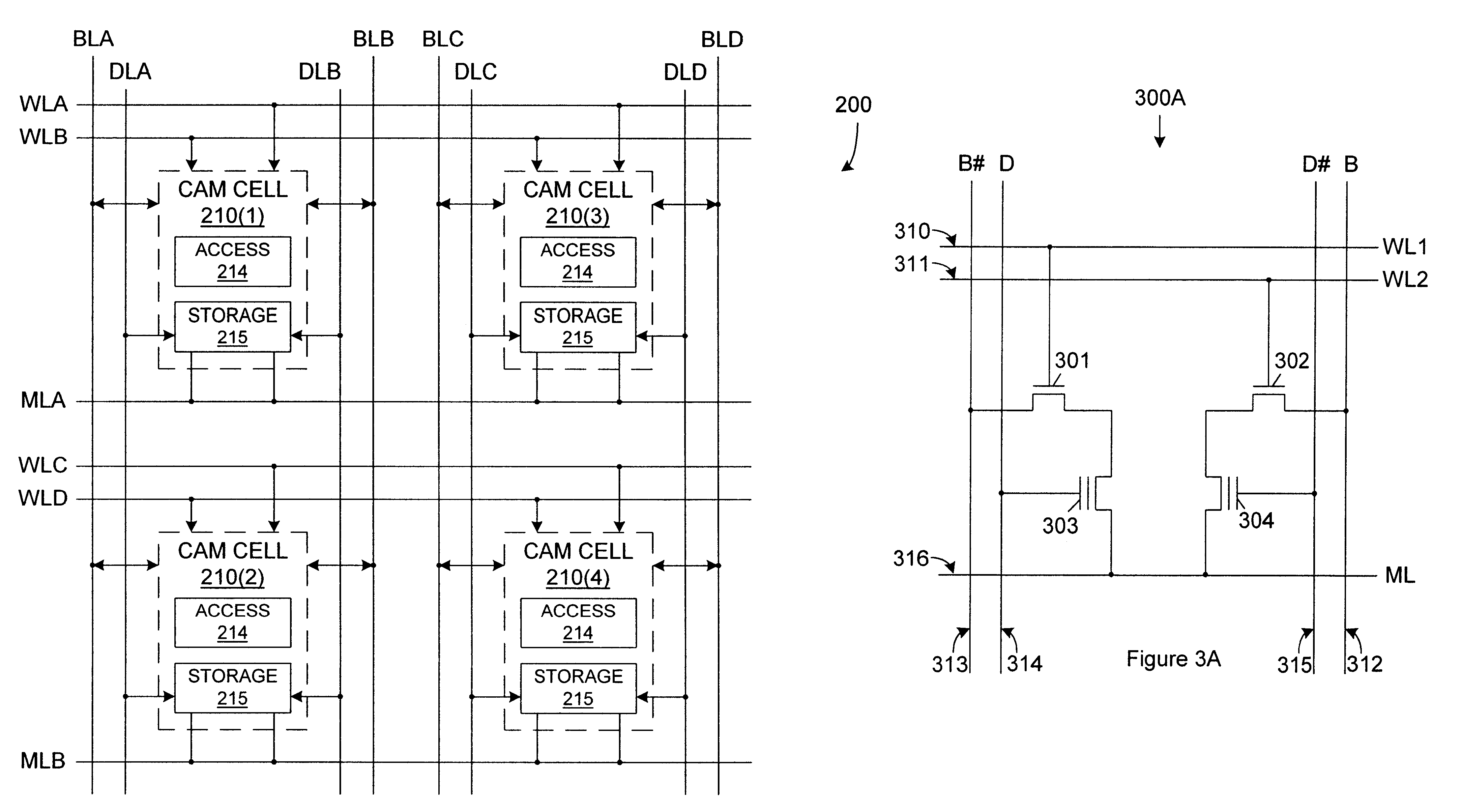
FIG. 3A is a schematic diagram of a novel four-transistor non-volatile ternary CAM cell 300A in accordance with an embodiment of the present invention. Ternary CAM cell 300A includes n-channel transistors 301-302 and non-volatile transistors 303-304. Transistors 301-302 have first terminals coupled to the first terminals (e.g., drains) of transistors 303-304, respectively. Word lines 310-311 are coupled to the gates of transistors 301-302, respectively. An inverted bit line 313 is coupled to a second terminal of transistor 301. A bit line 312 is coupled to a second terminal of transistor 302. A data line 314 is coupled to a gate of transistor 303. An inverted data line 315 is coupled to a gate of transistor 304. A match line 316 is commonly coupled to the second terminals (e.g., sources) of transistors 303-304.

The operation of ternary CAM cell 300A will now be described. During normal operation, CAM cell 300A is placed in various conditions, including standby...


PUM


Abstract

A CAM array includes non-volatile ternary CAM cells that use access transistors to easily read from and write to the non-volatile transistors. Each ternary CAM cell includes a pair of storage elements that are used to store a data bit value, and an access element that is used during CAM array operation. During a comparison operation, when the applied data value matches the stored value, the storage elements de-couple the match line from a discharging bit line (i.e., a high voltage on the match line remains high). Conversely, when the applied data value does not match the stored value, the storage elements couple the match line to a discharging bit line, thereby discharging the match line.

Description

The present invention relates to content addressable memory (CAM) arrays. More specifically, the present invention relates to ternary CAM cells and methods for operating these cells in a CAM array.DISCUSSION OF RELATED ARTUnlike conventional random access memory (RAM) arrays, CAM arrays include memory cells that are addressed in response to their content, rather than by a physical address within a RAM array. That is, data words stored in a RAM array are accessed by applying address signals to the RAM array input terminals. In response to each unique set of address signals, a RAM array outputs a data value that is read from a portion of the RAM array designated by the address. In contrast, a CAM array receives a data value that is compared with all of the data values stored in rows of the CAM array. In response to each unique data value applied to the CAM array input terminals, the rows of CAM cells within the CAM array assert or de-assert associated match signals indicating whether ...

Claims


Application Information

Patent Timeline
IPC IPC(8): G11C15/00G11C15/04
CPCG11C15/046
Inventor LIEN, CHUEN-DERWU, CHAU-CHIN
Owner AVAGO TECH INT SALES PTE LTD
Why Eureka
Try Eureka