
Image forming apparatus having float electrode provided to make uniform electric field

Inactive Publication Date: 2001-09-04
SHARP KK
View PDF5 Cites 0 Cited by
  • Summary
  • Abstract
  • Description
  • Claims
  • Application Information

AI Technical Summary

Benefits of technology

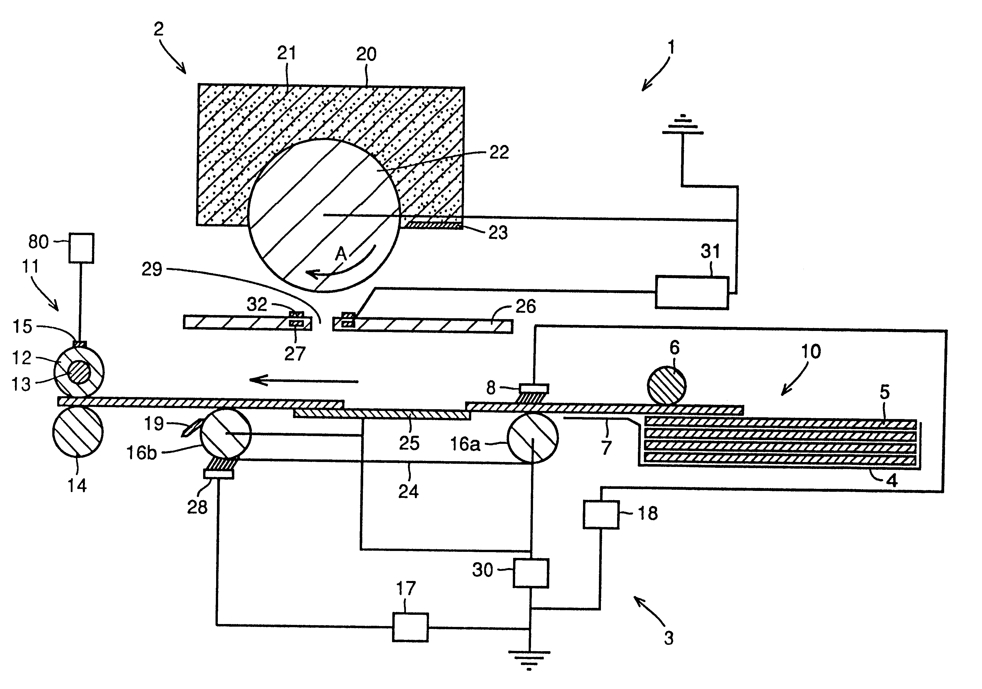
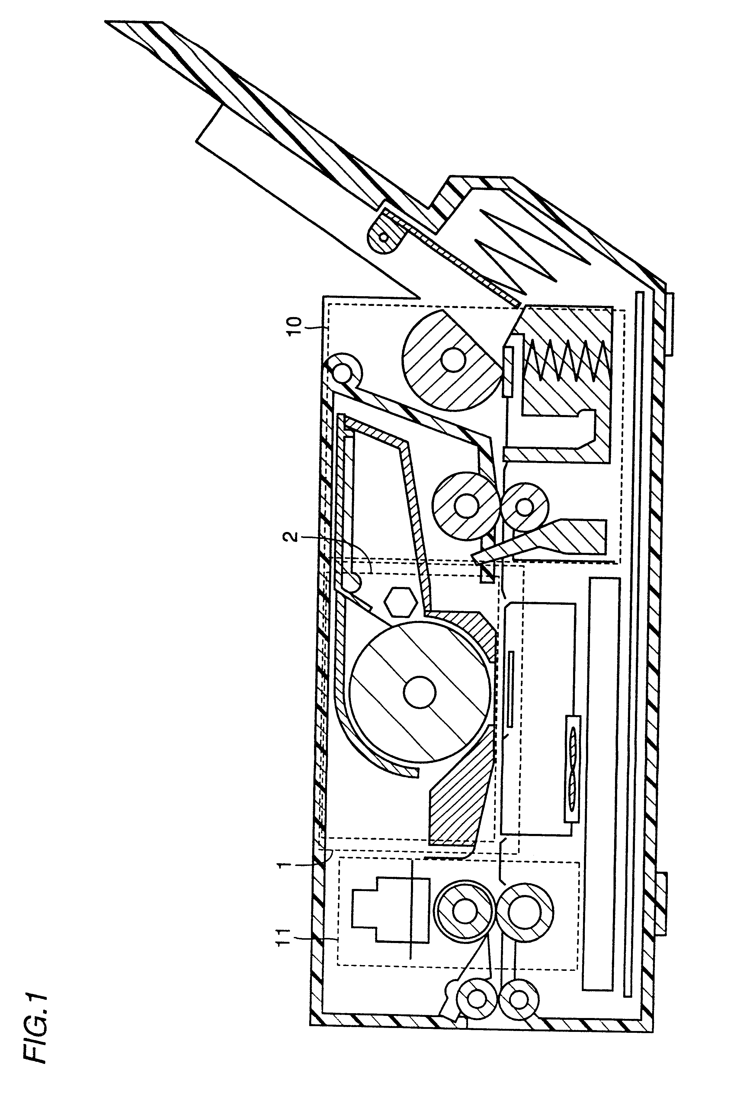
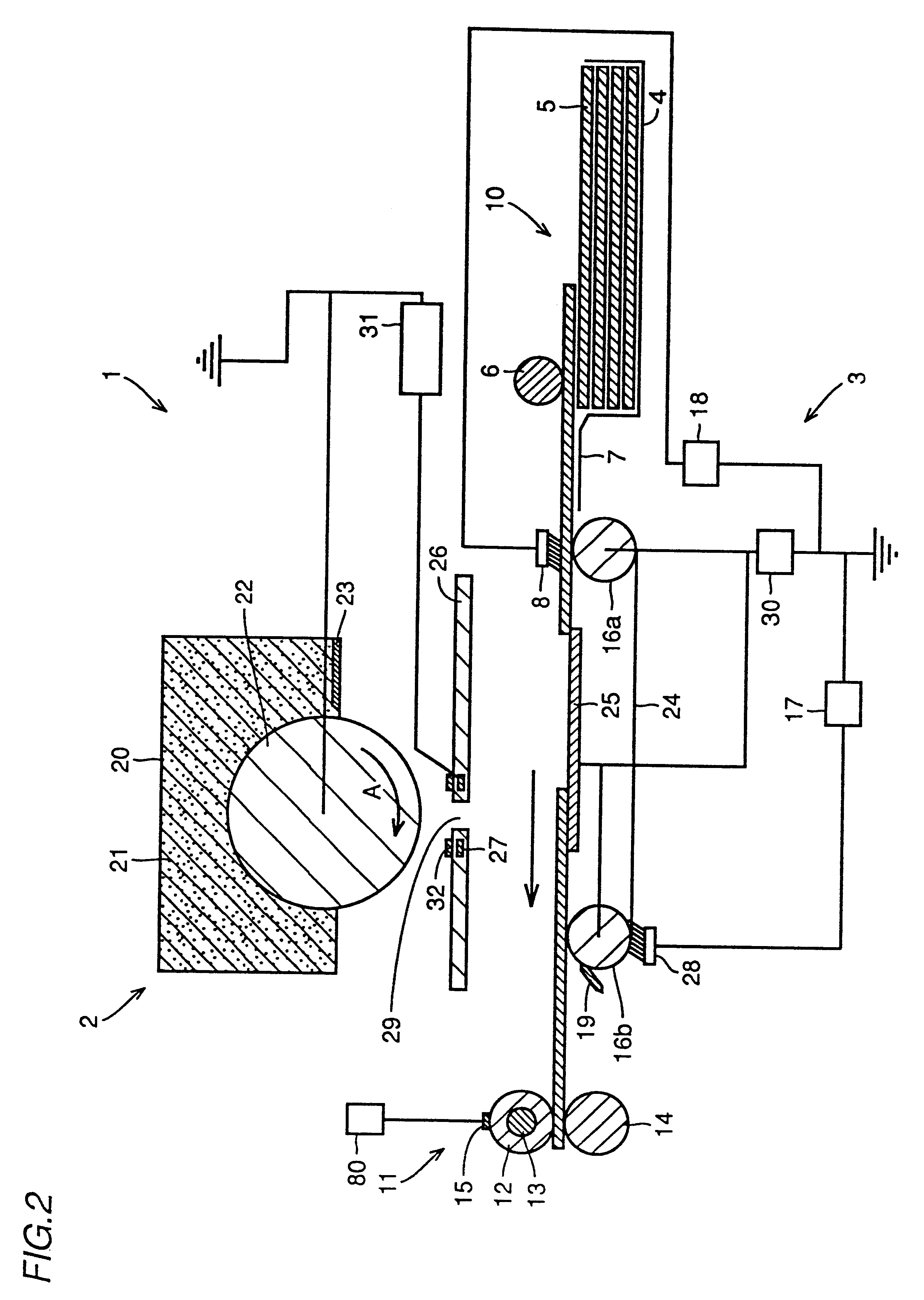
As the float electrodes are utilized, unevenness of the electric field between the control electrode and the toner carrier can be avoided without using any special circuit, and hence the electric field can be made uniform by a simple structure. In this manner, image formation with uniform density becomes possible, and it becomes possible to reduce the number of parts, the size of the apparatus and the cost.
By providing float electrodes and adjusting thickness of the float electrodes in accordance with the present invention, electric field strength between the control electrode and the toner carrier can be made constant even when the distance therebetween varies, and hence unevenness of the electric field can be avoided, without changing the structure of the insulating substrate itself.
By adjusting the positions of the float electrodes, it becomes possible to change relative positional relation between the control electrode and the toner carrier, and to control the electric field between the control electrode and the toner carrier. Thus, unevenness of the electric field can satisfactorily be avoided.
By controlling the thickness of the insulating substrate while not changing the thickness of the float electrodes, it is possible to control the electric field between the control electrode and the toner carrier, and unevenness of the electric field can satisfactorily be avoided.

Problems solved by technology

Therefore, the density of the dots formed at the end portion is low, resulting in unsatisfactory contrast, while the dot density is high at the central portion.
This unavoidably leads to increased cost of FETs as well as of necessary measure for insulating the circuit from the high voltage.
Therefore, the number of parts and the size of the apparatus are unavoidably increased.
Therefore, when a high potential is applied as a potential preventing jetting (hereinafter referred to as OFF potential), then a potential necessary for jetting (hereinafter referred to as ON potential) must be set sufficiently low, which prevents satisfactory jetting of the developer, resulting in blurred image with low contrast.
Conversely, when a high potential is applied as the ON potential, the OFF potential must be set sufficiently low and, in that case, prevention of jetting of the developer will be insufficient, causing a fog.
Accordingly, satisfactory contrast cannot be obtained, resulting in poor image formation.
Further, in a color image forming apparatus, not only dot formation but also color reproductivity are degraded as desired toner jetting cannot be ensured.
As a result, image quality degrades.
This unavoidably leads to increased cost and size of the apparatus, as the number of parts is increased.
However, it is difficult to arrange the carrier and the insulating substrate with high precision.
If the arrangement is not sufficiently precise, it is possible that the insulating substrate comes into contact with the surface of the toner carrier, destroying a developer layer carried thereon.
In that case, in addition to the problems described above, the state of the developer layer could be changed, and therefore desired control of developer jetting is impossible, preventing satisfactory image formation.
Further, in this case also, color reproduction would be insufficient in a color image forming apparatus, resulting in image degradation.
Therefore, such arrangement of the insulating substrate in a practical apparatus has been difficult.
This makes the apparatus complicated and increases the number of parts and cost.
In addition, if it becomes necessary to provide ICs for controlling the control electrodes on both surfaces as interconnections are provided on both surfaces of the insulating substrate, attachment of the apparatus to an image forming mechanism would be difficult as compared with attachment simply on one surface.

Method used


Image

  • Image forming apparatus having float electrode provided to make uniform electric field
  • Image forming apparatus having float electrode provided to make uniform electric field
  • Image forming apparatus having float electrode provided to make uniform electric field

Examples


second embodiment

Float electrode 32 in accordance with the second embodiment will be described. FIG. 9 shows float electrodes 32 each having a polygonal shape. By changing the shape, it is possible to change the electric field strength between float electrode 32 and toner carrier 22. More specifically, by changing the shape of the control electrode, the area from which the electric field is generated is changed, and accordingly, the strength of the electric field is changed. By using the control electrode in place of the circular control electrode shown in FIG. 5, more appropriate electric field control is possible.

In FIG. 9, a method is shown in which the shape of the electrode surface is changed. The change is not limited, however, to two-dimensional shape of the electrode structure. For example, the electrode shape may be changed three-dimensionally. The method of changing the structure is not specifically limited.

third embodiment

FIG. 10 shows a third embodiment in which float electrodes 32 have different thicknesses. As already described with respect to the principal of operation, the electric field strength changes in proportion to the change in distance between the surface of the float electrode 32 and the toner carrier 22. Therefore, if the electric field strength between the surface of float electrode 32 and toner carrier 22 is to be increased, it is possible by making thicker the float electrode 32. When toner carrier 22 has a curvature as shown in FIG. 10, the distance between the surface of float electrode 32 and toner carrier 22 differs at an end portion and at the central portion. Therefore, the difference in distance can be adjusted by changing the thickness of float electrodes 32. When the distance between centers of the gates at the end portion and at the central portion is 2 mm and the diameter of toner carrier 22 is 30 mm, the developed image comes to have approximately the same density at the...

fourth embodiment

FIG. 11 shows a fourth embodiment of the float electrodes 32. In the method in which thickness of float electrodes 32 is made different described above, it may be difficult to control the thickness dependent on the manufacturing method of the electrode. In such a case, the insulating substrate may be formed in several layers, and by arranging float electrodes 32 having the same thickness at different layers of insulating substrate, similar effect as described above can be obtained.


PUM


Abstract

An image forming apparatus capable of forming an image with uniform density includes a toner carrier for carrying a toner, an opposing electrode arranged opposing to the toner carrier, a high voltage power supply unit for supplying a voltage to generate a potential difference between the toner carrier and the opposing electrode, a control electrode including a plurality of electrodes arranged between the toner carrier and the opposing electrode, and a control power supply unit for implementing a plurality of potential states at respective ones of the electrodes of the control electrode, controlling passage of the toner through a passage portion, and for forming an image on a surface of a recording medium conveyed over the opposing electrode. The control electrode includes an insulating substrate, the aforementioned plurality of electrodes having a passage portion through which the toner passes provided in the insulating substrate, and a plurality of float electrodes having an opening provided such that at least part of the plurality of electrodes are directly or electrically exposed to the toner carrier, for making uniform an electric field formed between the toner carrier and the opposing electrode.

Description

1. Field of the InventionThe present invention relates to an image forming apparatus applied to a printing unit of a digital copying machine, a facsimile or the like as well as to a digital printer, a plotter or the like, for forming an image on a recording medium by jetting a developer.2. Description of the Background ArtAn image forming apparatus outputting image signals as a visible image on an recording medium such as a sheet of paper has been known, as disclosed, for example, in Japanese Patent Laying-Open No. 6-91918. In the image forming apparatus, an electric field is exerted on charged particles so that the particles jet out or travel by the electric force, and by changing potentials applied to a control electrode including a plurality of passage holes arranged along the jet travel path, the charged particles are attracted and adhered on the recording medium, whereby the image is directly formed on the recording medium.Another image forming apparatus has also been proposed ...

Claims


Application Information

Patent Timeline
IPC IPC(8): B41J2/41B41J2/415B41J2/385G03G15/05
CPCB41J2/4155G03G2217/0025
Inventor IMAIZUMI, DAISAKUNISHIO, YUKIHITOFUJITA, HIROKAZUWAKAHARA, SHIROU
Owner SHARP KK
Learn More