
Touchpad device and manufacturing method thereof

a technology of touchpad and manufacturing method, which is applied in the field of input devices, can solve the problems of time-consuming and inconvenient manufacturing process, easy overflow of adhesive, and easy uneven application of liquid adhesive, and achieves faster curing speed, improved flatness, and thin thickness.

Active Publication Date: 2022-10-27
CHICONY ELECTRONICS
View PDF11 Cites 0 Cited by
  • Summary
  • Abstract
  • Description
  • Claims
  • Application Information

AI Technical Summary

Benefits of technology

The present patent is about a new method and device for manufacturing a touchpad device. The method uses a light-curing adhesive film instead of liquid adhesive, which reduces the time-consuming and inconvenient process and prevents the adhesive from overflowing. The adhesive film is also thinner and faster curing, which prevents bubbles and ensures better flatness and reduced thickness of the finished device. The cured adhesive film provides better rigidity to prevent touch panel deflection or bending when pressed. Overall, the present invention offers an improved manufacturing method for touchpad devices.

Problems solved by technology

As a result, the manufacturing process is time-consuming and inconvenient.
Additionally, during attaching the circuit board to the liquid adhesive, overflow of adhesive may occur easily.
Moreover, the applied liquid adhesive has a larger thickness (the thickness of the applied liquid adhesive is at least 0.15 mm) and uneven application of the liquid adhesive may occur easily.
Furthermore, during the high-temperature baking procedure, bubbles may be formed in the liquid adhesive.
Therefore, following issues are generated: unevenness of the touch panel, limitation in the reduction of the overall thickness of the touchpad device, adverse effect on the pressing feeling of the user, poorer rigidity of the component assembled by the touchpad and the circuit board, in which when the corner of the touch panel is pressed, the touch panel may have deflection or bending or may have an excessive idle stroke.

Method used


Image

  • Touchpad device and manufacturing method thereof
  • Touchpad device and manufacturing method thereof
  • Touchpad device and manufacturing method thereof

Examples


Embodiment Construction

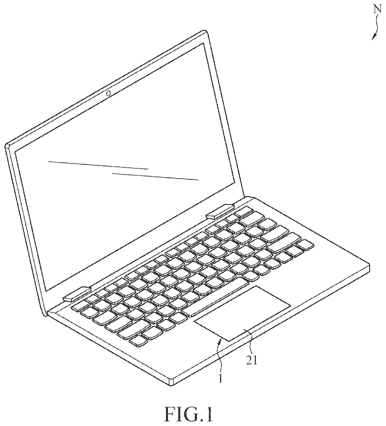
[0019]FIG. 1 illustrates a schematic application view of a touchpad device according to an exemplary embodiment of the instant disclosure. As shown in FIG. 1, the touchpad device 1 may be applied in a computer product, and the user can operate the touchpad device 1 by sliding or pressing the touchpad device 1 with the user's finger(s) so as to control the movement of the cursor or to generate corresponding control signal(s). For example, in this embodiment, the touchpad device 1 is applied in a notebook computer N, but embodiments are not limited thereto. In some embodiments, the touchpad device 1 may be applied in other portable computers (e.g., tablet computers). Alternatively, the touchpad device 1 may be an individual device and may be capable of externally connected to a portable computer, but embodiments are not limited thereto.

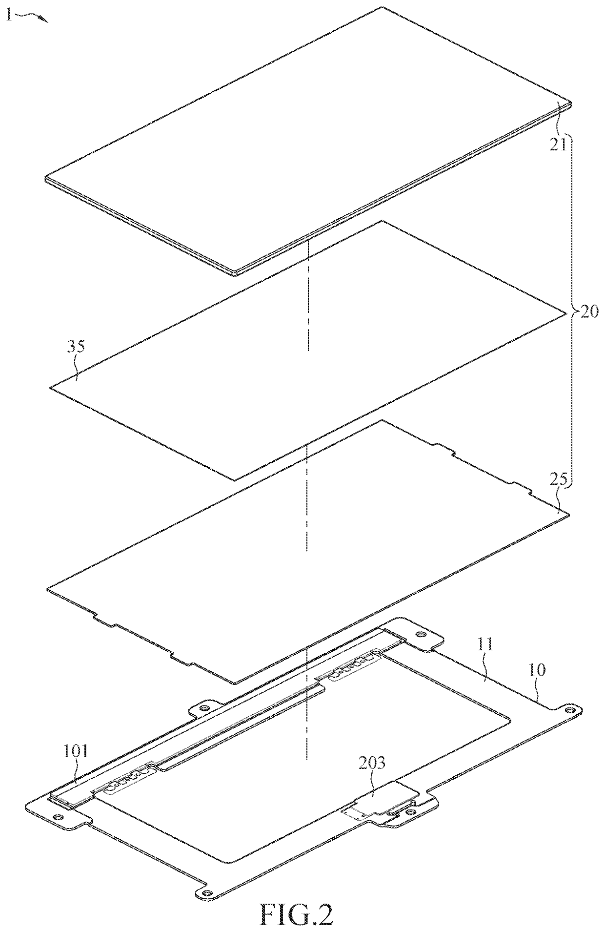
[0020]FIG. 2 illustrates an exploded view of the touchpad device of the exemplary embodiment. FIG. 3 illustrates a cross-sectional view of the touchpad...


PUM


Abstract

A touchpad device includes a substrate, a touch panel, and a light-curing adhesive film. The substrate includes a top surface, the touch panel is disposed above the top surface of the substrate, and the touch panel includes a touchpad and a circuit board stacked with each other. The light-curing adhesive film is bonded between the touch board and the circuit board, and the light-curing adhesive film is in a cured state.

Description

CROSS-REFERENCE TO RELATED APPLICATION[0001]This non-provisional application claims priority under 35 U.S.C. § 119(a) to Patent Application No. 110114595 filed in Taiwan, R.O.C. on Apr. 22, 2021, the entire contents of which are hereby incorporated by reference.BACKGROUNDTechnical Field[0002]The instant disclosure relates to an input device, in particular, to a touchpad device and manufacturing method thereof.Related Art[0003]Touchpads are common input devices widely applied in computers. The touchpad is provided for sensing the movement or pressing of a user's finger(s) to control the cursor to perform an action (e.g., to move, to click, or the like).SUMMARY[0004]A manufacturing method of touchpad device known to the inventor includes applying a liquid adhesive on a touch panel by an adhesive dispenser, attaching a circuit board to the adhesive, and then applying a high-temperature baking procedure to fix the touch panel with the circuit board by the adhesive.[0005]However, in the ...

Claims


Application Information

Patent Timeline
IPC IPC(8): G06F3/0354
CPCG06F3/03547
Inventor HOU, PO-CHUNLI, PO-HSIN
Owner CHICONY ELECTRONICS
Learn More