Resin card medium and manufacturing method therefor

a technology of resin card and medium, which is applied in the direction of casings/cabinets/drawers, casings with display/control units, instruments, etc., can solve the problems of affecting the appearance and printability of the ic card, deteriorating flatness and smoothness, and easy breakage of electronic components, etc., to achieve restrain card deformation, and unevenness of molten plasti

Active Publication Date: 2022-09-13
SHOEI INSATSU +1
View PDF17 Cites 0 Cited by
  • Summary
  • Abstract
  • Description
  • Claims
  • Application Information

AI Technical Summary

Benefits of technology

[0037]According to the present invention, since the temperature upon hot pressing is managed at the temperature which is the softening point or more of the plastic fibers in the mixed paper and less than the melting point thereof, excellent effect in that the plastic fibers in the mixed paper neither melt nor a sink and warpage of the card medium are caused due to the solidification speed unevenness of the molten plastic can be obtained. In other words, excellent effect in that the sink and the warpage of the card medium caused due to the curing speed unevenness of the softened plastic fibers are much smaller than the sink and the warpage of the card medium caused due to the solidification speed unevenness of the molten plastic can be obtained.
[0038]According to the present invention, since the plant fibers whose shape, nature, and the like hardly change even if the influence of heat is exerted thereon are contained in the mixed paper, excellent effect in that flowing of the softened resin is inhibited, and even if the residual stress in the card is caused due the curing speed unevenness or the like of the plastic fibers, the plant fibers serve as the reinforcing material and deformation of the card is restrained, and as a result, the release of the residual stress is prevented, thereby preventing the warpage and the deformation of the card can be obtained.
[0039]In addition, according to the present invention, since upon hot pressing, the mixed paper constituted of the plastic fibers and the plant fibers functions as the cushion material, the mixed paper absorbs the thickness or thicknesses of the electronic component or electronic components so as to keep the flatness of the card medium after molding. As described above, in order for the mixed paper to surely absorb the thickness or thicknesses of the electronic component or electronic components, it is preferable that the percentage of the total of the thickness of the substrate and the thickness or thicknesses of the electronic component or electronic components to the thickness of the card medium after the hot pressing molding is adjusted to be 80% or less, and it is more preferable that the percentage of the total of the thickness of the substrate and the thickness or the thicknesses of the electronic component or electronic components to the thickness of the resin card medium after the hot pressing molding is adjusted to be 70% or less. As a result of this, according to the present invention, the resin card medium having extremely excellent flatness and smoothness in that the card warpage amount of the resin card medium of the present invention in conformity with the ISO / IEC 7810:2003 standard is 1.5 mm or less and besides the ISO standard, the depth of the card local depressed part thereof is less than 0.2 mm can be obtained.

Problems solved by technology

Therefore, on a surface pf the IC card including these, a projecting portion is formed due to the thickness of the electronic component such as the IC chip, thereby deteriorating flatness and smoothness.
In addition, if an external force is exerted on the projecting portion formed by the electronic component, the problem in that the electronic component is easily broken arises.
Furthermore, appearance and printability of the IC card are impaired, thereby also leading to the problem in that an appearance commercial value is reduced.
However, in the incorporating method described in Patent Literature 1, it is required to change a shape and a placement position of the depressed part or the hole of the paper layer in accordance with a shape and a placement position of the electronic component on the substrate, thereby leading to the problem in that extremely burdensome processes are required and costs are also increased.
However, in the incorporating method described in Patent Literature 2, since the adhesive layer (hot melt layer) on the electronic component on the surface of the substrate is melt once, there arises the problem in that due to solidification speed unevenness upon curing resin, a sink is caused, a sufficient degree of flatness cannot be thereby obtained, or warpage is easily caused.
In addition, there is a risk of damaging the electronic component due to an influence of heat, thereby also leading to the problem in that an electronic component to be used is limited only to an electronic component having heat resisting properties to some extent.
However, in the method described in each of Patent Literatures 3 and 4, since the resin with which the fibers or the fiber sheet is impregnated is in a molten state, shrinkage unevenness of the fibers or the fiber sheet is caused or promoted due to the solidification speed unevenness upon curing the resin, thereby resulting in the problem in that warpage of the card becomes large.
In particular, there arises the problem in that when the electronic component or the substrate on which the electronic component is mounted is displaced to either one of a front side or a rear side of the card, the warpage of the card tends to become further large.

Method used


Image

  • Resin card medium and manufacturing method therefor
  • Resin card medium and manufacturing method therefor
  • Resin card medium and manufacturing method therefor

Examples


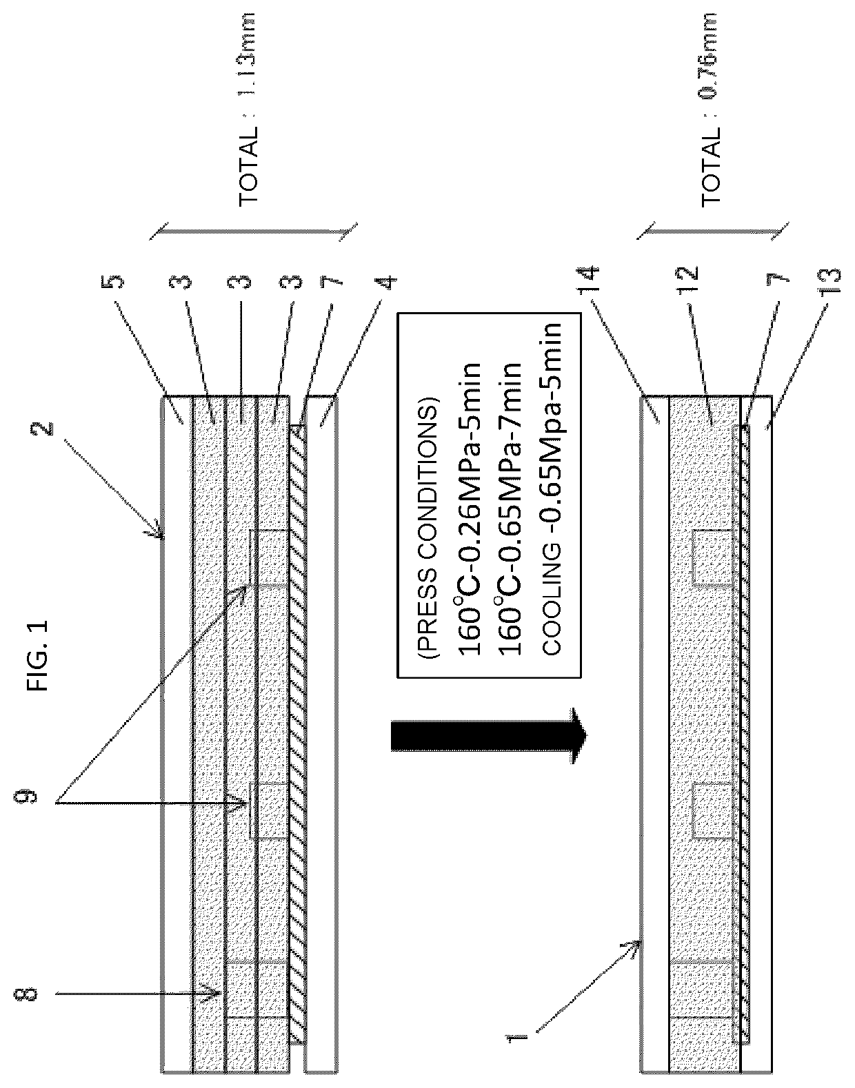
example 1 (see fig.1)

Example 1 (See FIG. 1)

[0056](1) Card Medium Laminated Body

[0057]On a substrate 7 (with a product name “Polyimide Substrate”) having a size of 35 mm×78 mm and a thickness of 0.10 mm, one plastic pseudo chip A (8) having a 7-mm-square size and a thickness of 0.4 mm and two plastic pseudo chips B (9) each having a 7-mm-square size and a thickness of 0.25 mm were arranged in appropriate positions, thereby preparing a substrate 7 having the pseudo chips 8 and 9 installed thereon.

[0058]Next, one first finishing sheet 4 (with a product name “DIAFIX PG-WHI-FG”, manufactured by Mitsubishi Plastics, Inc., having a thickness of 0.20 mm and a melting point of 80° C.) formed of polyethylene terephthalate glycol-modified (PETG) was prepared; on the first finishing sheet 4, the above-mentioned substrate 7 was laminated with a side, on which the pseudo chips 8 and 9 were installed, facing upward; three pieces of mixed paper 3 (with a product name “SC-01”, manufactured by TOMOEGAWA CO., LTD., having...

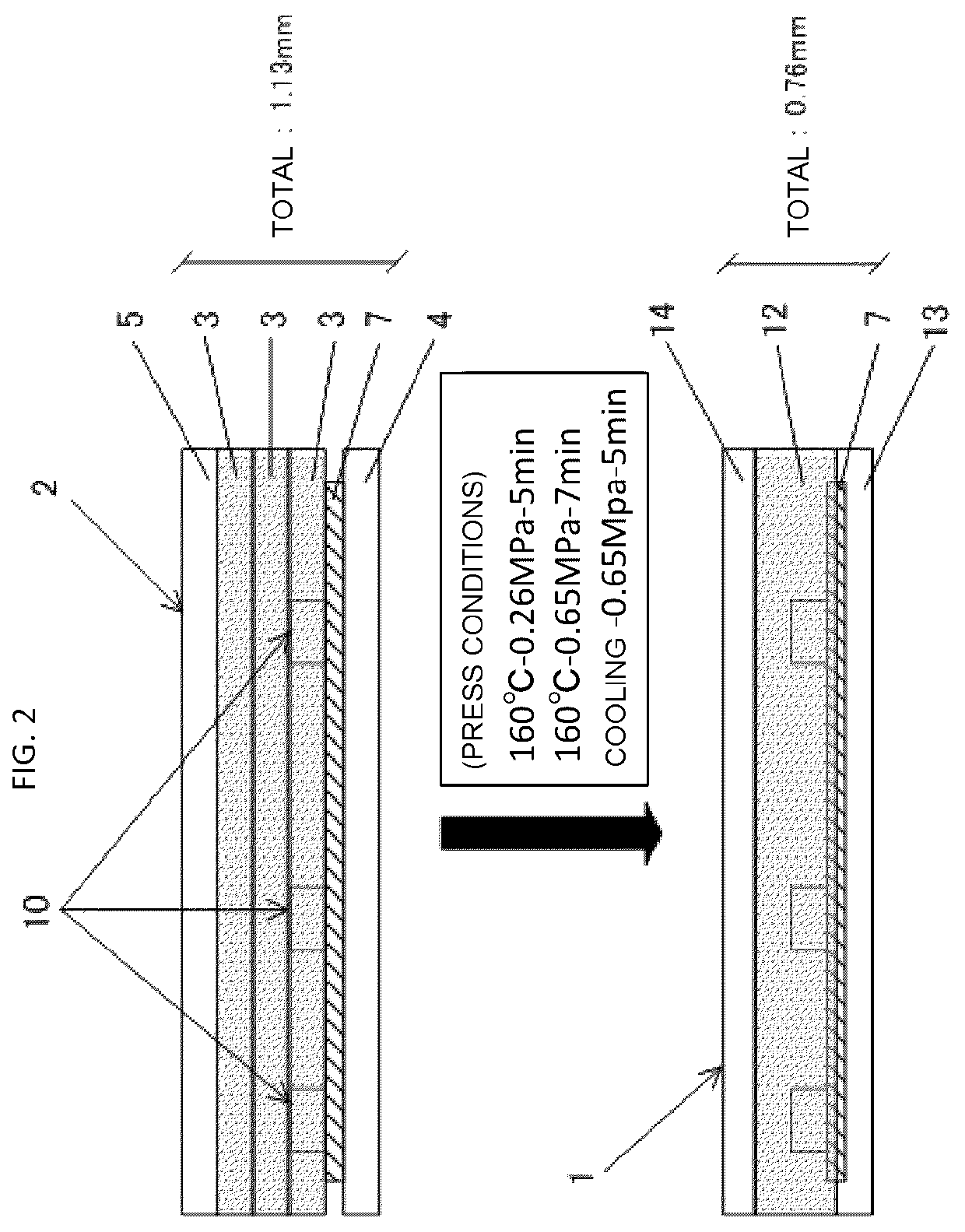
example 2 (see fig.2)

Example 2 (See FIG. 2)

[0061](1) Card Medium Laminated Body

[0062]The same configuration as that in Example 1 except that three plastic pseudo chips C (10) each having a 7-mm-square size and a thickness of 0.2 mm were used and arranged in appropriate positions on a substrate 7 was employed, thereby forming a card medium laminated body 2 in Example 2.

[0063](2) Hot Pressing Molding

[0064]The card medium laminated body 2 in Example 2 was subjected to hot pressing molding under the same conditions as those in Example 1, thereby preparing a resin card medium 1 in Example 2 whose shape and dimensions were in conformity with the ISO / IEC 7810:2003 standard.

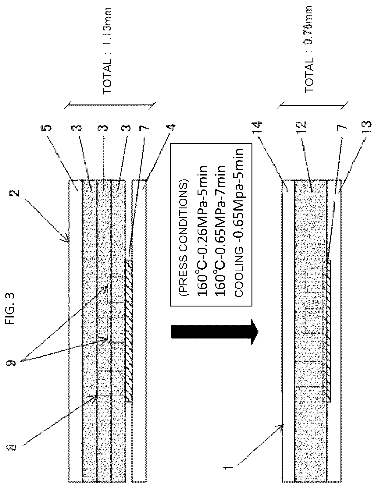
example 3 (see fig.3)

Example 3 (See FIG. 3)

[0065](1) Card Medium Laminated Body

[0066]The same configuration as that in Example 1 except that a substrate 7 (with a product name “Polyimide Substrate”) having a size of 35 mm×40 mm and a thickness of 0.10 mm was used was employed, thereby forming a card medium laminated body 2 in Example 3.

[0067](2) Hot Pressing Molding

[0068]The card medium laminated body 2 in Example 3 was subjected to hot pressing molding under the same conditions as those in Example 1, thereby preparing a resin card medium 1 in Example 3 whose shape and dimensions were in conformity with the ISO / IEC 7810:2003 standard.


PUM

PropertyMeasurementUnit
depthaaaaaaaaaa
depthaaaaaaaaaa
thicknessaaaaaaaaaa

Abstract

A resin card medium which has a substrate having electronic components mounted thereon and has sophisticated flatness and smoothness realized without providing any layer having holes for absorbing thicknesses of the electronic components; and a method for manufacturing a resin card medium.A resin card medium laminated body before pressing is prepared by laminating, on a first plastic finishing sheet, a substrate having one electronic component or two or more electronic components installed on one side of the substrate, with the one side, on which the electronic component or electronic components are installed, facing upward, and laminating, on the substrate, mixed paper constituted of plastic fibers and plant fibers, and by subjecting the resin card medium laminated body to hot pressing at a temperature which is a softening point or more of the plastic fibers and less than a melting point of the plastic fibers.

Description

TECHNICAL FIELD[0001]The present invention relates to a resin card medium, which includes an electronic component or electronic components such as an IC chip or IC chips and is flat and smooth, and a manufacturing method therefor and, in particular, to a resin card medium which is obtained by laminating mixed paper on a surface of a substrate on a side on which the electronic component or electronic components are mounted and by conducting hot pressing therefor, has a card warpage amount thereof in conformity with an ISO / IEC 7810:2003 standard of 1.5 mm or less, and besides the above-mentioned ISO standard, achieves a depth of a card local depressed part thereof of less than 0.2 mm, and a manufacturing method therefor.BACKGROUND ART[0002]In recent years, in order to meet the demands for high functionality, multi-functionality, enhancement in security performance, and the like, it is often the case that a substrate on which electronic components such as an IC (Integrated Circuit) chi...

Claims


Application Information

Patent Timeline
Patent Type & Authority Patents(United States)
IPC IPC(8): H05K5/06B32B27/08B32B27/20B32B27/28B32B27/36B32B37/10H05K5/00
CPCH05K5/065B32B27/08B32B27/20B32B27/281B32B27/36B32B37/10H05K5/0017B32B2457/00B42D25/305B42D25/455B42D25/46B42D25/36B42D25/23G06K19/07722B32B2262/06B32B2262/14B32B5/02B32B2262/0284B32B29/005B32B2307/734B32B27/10B32B27/12B32B3/085B32B2262/02B32B2307/732B32B37/0015
Inventor NAKATA, TOMOHIROMORIUCHI, HIDEKI
Owner SHOEI INSATSU
Why Eureka
Try Eureka