

Electron source and production thereof and image-forming apparatus and production thereof
- Summary
- Abstract
- Description
- Claims
- Application Information
AI Technical Summary
Problems solved by technology
Method used
Image

Examples
embodiment 1
Embodiment 1 of the present invention is described by reference to FIGS. 1 to 10.
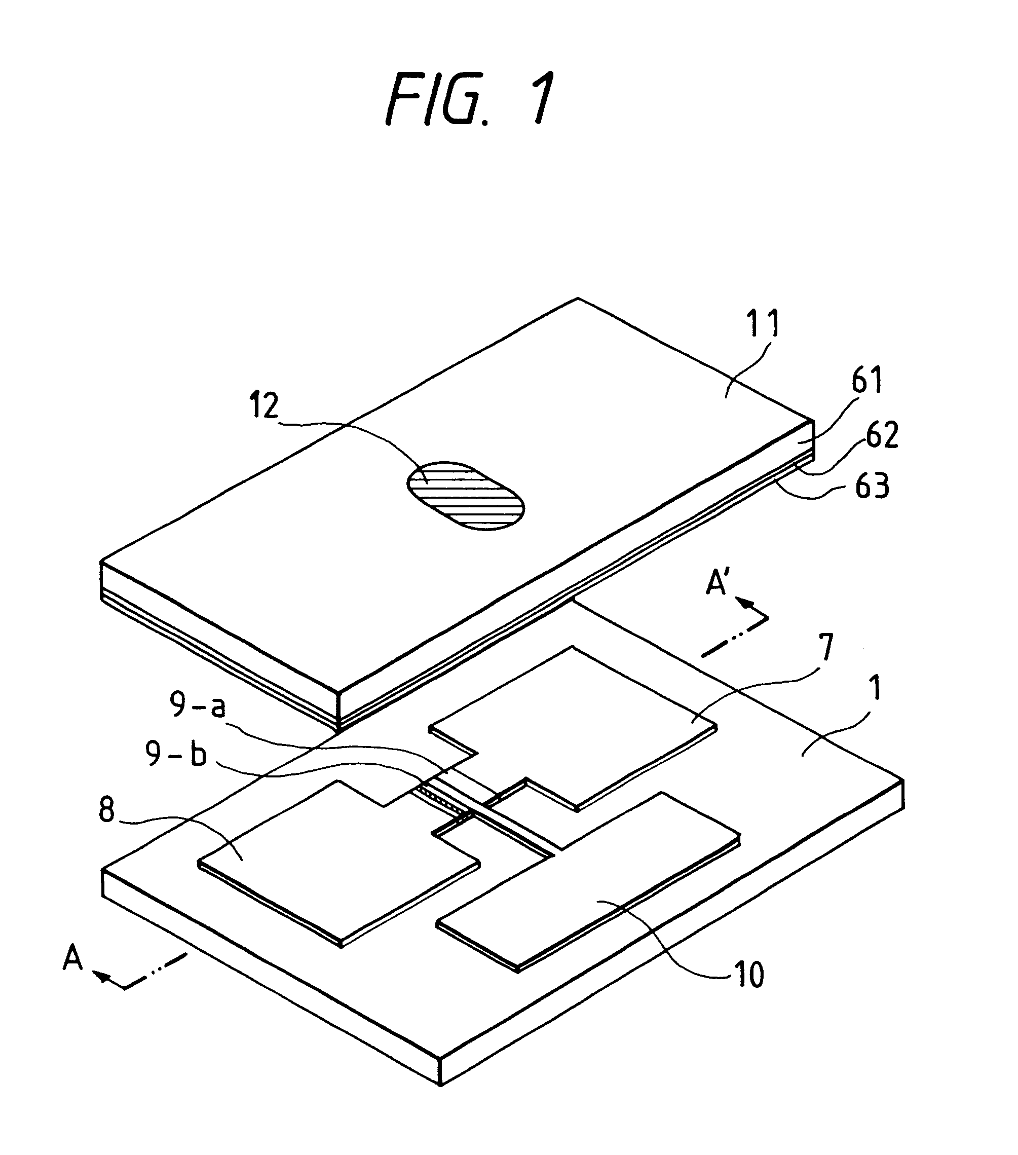
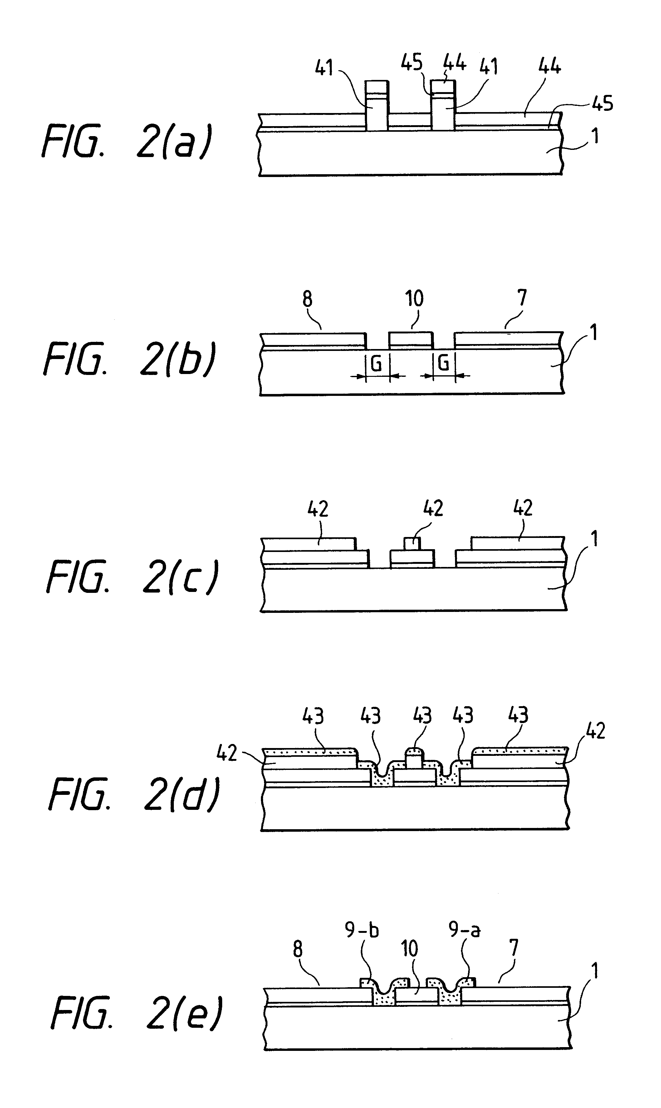
FIG. 1 is a perspective view of a portion of a display device of the present invention, showing one of surface conduction emitting elements as an electron source and a face plate comprising a fluorescent substance as an image-forming member. The surface conduction emitting element in FIG. 1 is constructed of an insulating substrate 1, (e.g., made of glass), electrodes 7,8, thin films 9-a, 9-b, for electron-emitting region formation (electron-emitting region formed in 9-b), and a selecting electrode 10. The face plate 11 of the display device is constructed of a light-transmissive plate 61 (e.g., made of glass), having on the inside face thereof a metal back 63 and a fluorescent material 62 generally known for CRT use. Further, under the fluorescent material 62, a light-transmissive electrode, (e.g., made of an ITO thin film) may be provided which are known in the application field of CRT. A voltage (e.g...
embodiment 2
A second embodiment of the present invention is described by reference to FIGS. 11 to 14.
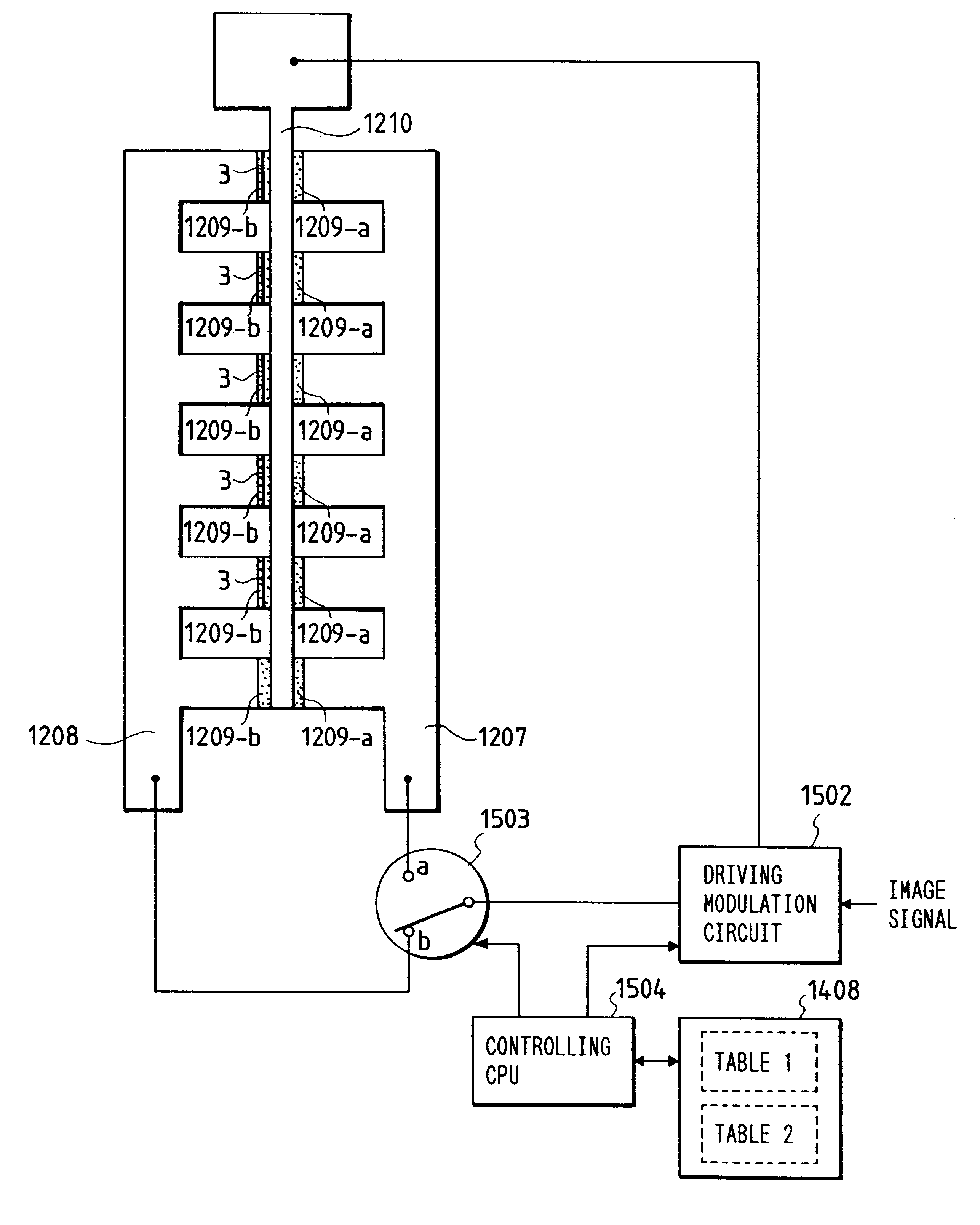
FIG. 11 is a plan view of this type of a surface conduction electron-emitting element. The element comprises element electrodes 1207, 1208, emitting region-generating thin films 1209-a, 1209-b, and selecting electrode 1210. As is clear from the drawing, six emitting region-generating thin films are provided respectively for the 1209-a side and for the 1209-b side, namely twelve thin films in total. In the element of this embodiment, the element electrodes, the selecting electrode, and the emitting region-generating thin films are prepared in the same manner as described regarding the element in FIGS. 2(a) to 2(e). Therefore, the explanation thereof is omitted here.
In this embodiment, the emitting region-generating thin films are divided into two groups of 1209-a and 1209-b, each group of the thin films is tested for defectiveness and failure. The test may be conducted by the method using an imag...
embodiment 3
A third embodiment of the present invention is described by reference to FIGS. 15 to 21. This Embodiment is characterized in that a heat-fusible electroconductive member is employed as the means for changing the electric connection.
FIG. 15 illustrates this type of a surface conduction electron-emitting element before electrical forming treatment. The unit comprises a glass substrate 1, element electrodes 1601, 1602, an intermediate electrode 1603, an emitting region-generating thin film 1604, and a heat-fusible electroconductive member 1605. The portions of the emitting region-generating thin film 1604 on the both side of the intermediate electrode are named 1604-A and 1604-B, respectively.
The method of formation of the element unit is described by reference to the side views shown in FIGS. 16A(1) to 16A(3).
Firstly, as shown in FIG. 16A(1), element electrodes 1601, 1602, and an intermediate electrode 1603 are formed on a glass substrate. These electrodes can be formed readily by lam...
PUM
 Abstract
Description
Claims
Application Information