Driving circuit for display device

a display device and circuit technology, applied in static indicating devices, instruments, hydrocarbon distillation, etc., can solve the problems of increasing the size of the substrate, significant unsatisfactory display quality, and becoming remarkabl

Inactive Publication Date: 2001-12-11
SANYO ELECTRIC CO LTD
View PDF7 Cites 48 Cited by
  • Summary
  • Abstract
  • Description
  • Claims
  • Application Information

AI Technical Summary

Problems solved by technology

In particular, a significant uneveness in quality of display is caused by the distortion of the waveform on an end distant from an end where the original pixel signal is sent out or a central portion of a screen in a display section in which pixels are arranged in a matrix.
Furthermore, this problem has become remarkable with an increase in size of the substrate.
Therefore, distortion of data to be finally written to a pixel cannot be ignored.
Consequently, the quality of the display is deteriorated.
More specifically, if the difference between the previous pixel signal voltage and the subsequent pixel signal voltage is great, it takes a long time to change an original pixel signal voltage.
However, less effects are obtained by a further reduction in a sampling period...

Method used


Image

  • Driving circuit for display device
  • Driving circuit for display device
  • Driving circuit for display device

Examples


first embodiment

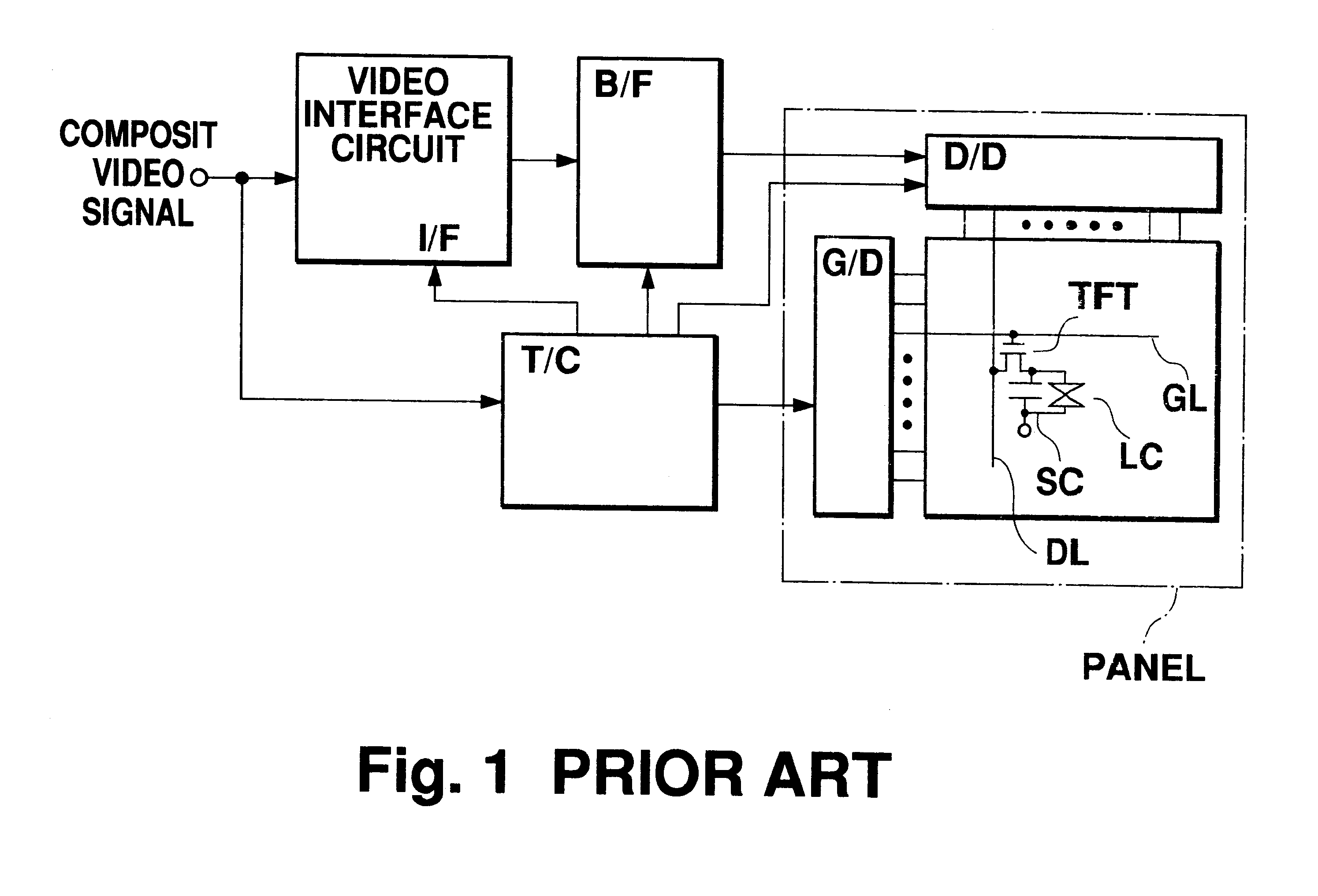
A driving circuit for an LCD according to the present invention has a structure shown in FIG. 4, and comprises the video interface circuit [I / F] 31 similar to [I / F] in FIG. 1, a buffer circuit [B / F] 32 for a drain driver [D / D] 36, and a timing controller [T / C] 33, wherein the video interface circuit 31 includes a signal waveform correcting circuit for correcting a signal distortion between . The drain driver 36 has the similar structure as in FIG. 2.

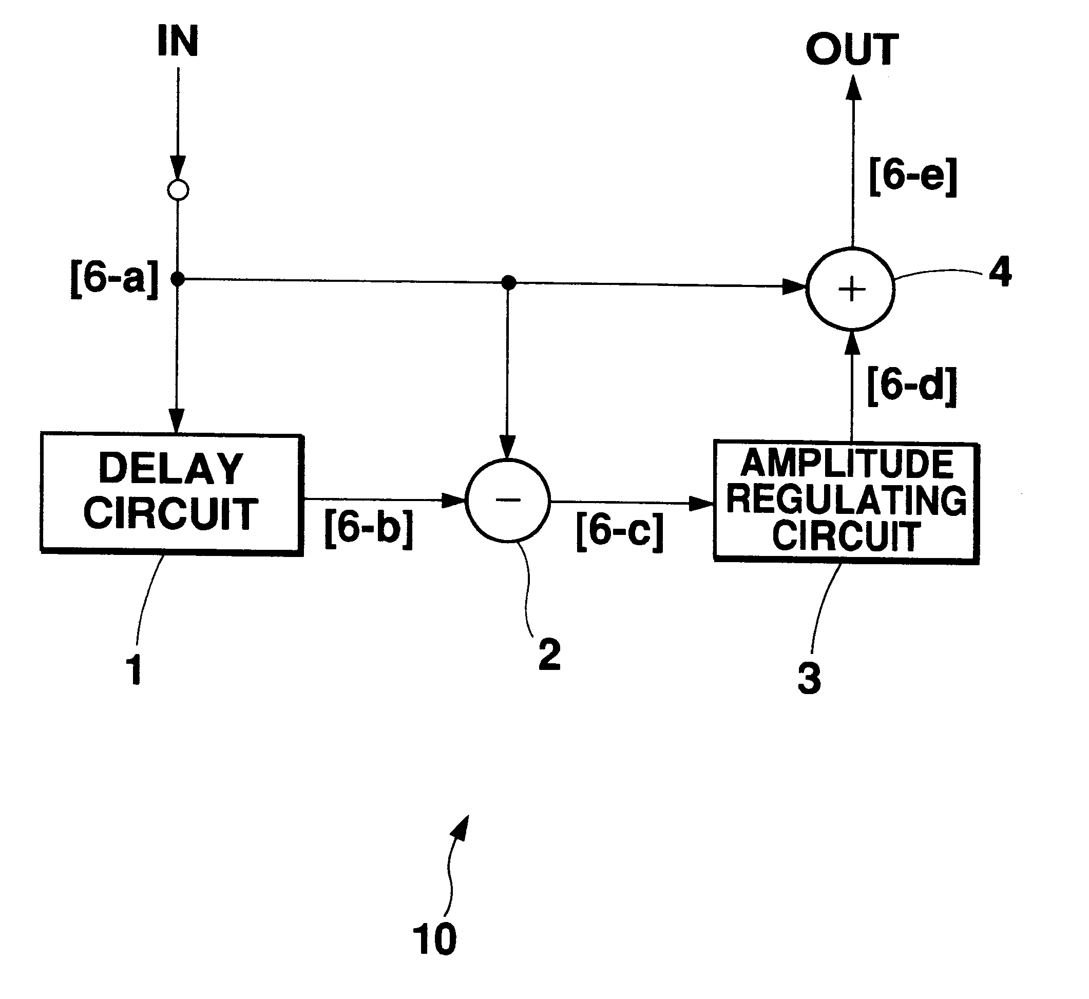
A structure of the signal waveform correcting circuit 10 includes a delay circuit 1, a subtracter 2, an amplitude regulating circuit 3 and an adder 4 as shown in FIG. 5. The signal waveform correcting circuit 10 may include the buffer circuit [B / F] 32 therein.

FIG. 6 shows a signal waveform in each path of FIG. 5.

An original pixel signal output from the interface circuit 31 is sent to the delay circuit 1, the subtracter 2 and the adder 4. In the delay circuit 1, a sent original pixel signal [6-a] is delayed by a predetermined quantity (ex...

second embodiment

While the overall structure of an LCD driving circuit according to a second embodiment is the same as in FIG. 4, a signal waveform correcting circuit 10 has the following structure and performs the following correction. FIG. 10 shows a structure of the signal waveform correcting circuit 10 according to the second embodiment.

The signal waveform correcting circuit 10 comprises a delay circuit 11, a subtracter 12, an amplitude amplifying circuit 13, an original pixel signal split circuit 14, a correction signal split circuit 15, and a selecting circuit 16. The delay circuit 11 delays an original pixel signal VD by m pixel periods corresponding to a split number m for the original pixel signal VD, for example, 4 pixel periods. A delay signal DL thus obtained is subjected to subtraction with the original pixel signal VD by the subtracter 12.

The amplitude amplifying circuit 13 amplifies or attenuates an amplitude of the original pixel signal VD with an amplification ratio corresponding to...

third embodiment

A more specific example of the structure of a signal processing section according to a third embodiment will be described below, in which the second embodiment is applied to an LCD using a p-SiTFT. FIG. 13 shows an example of the structure according to the third embodiment. The structure shown in FIG. 13 includes a path from the video interface circuit 31 to the drain driver 36 through the buffer circuit 32 shown in FIG. 4 in an LCD driving circuit. The case will be described in which each circuit shown in FIG. 13 is provided in the video interface circuit 31 shown in FIG. 4. In the third embodiment, the buffer circuit 32 shown in FIG. 4 is provided as a buffer circuit 55 in the video interface circuit 31.

Original pixel signals for color-decoded R, G and B are sent to an original pixel signal split--waveform correcting circuit (hereinafter referred to as a split correcting circuit) 100, through a contrast regulating circuit 50 and a .gamma.-correcting circuit 51, which is a feature ...


PUM


Abstract

A signal driving circuit for an active matrix type display device having display pixels arranged in a matrix, comprises a signal waveform correcting circuit receiving an input pixel signal for generating a corrected output pixel signal to the display device, said signal waveform correcting circuit including a delay circuit for generating a delay signal, a difference calculating circuit for calculating a difference signal between the input pixel signal and the delay signal, and a correction circuit for generating the corrected output pixel signal based upon the difference signal and the input pixel signal, wherein a portion of the waveform amplitude of the corrected output pixel signal is formed by adjusting a corresponding portion of the waveform amplitude of the input pixel signal based upon the difference signal.

Description

1. Field of the InventionThe present invention relates to a circuit and method for driving a display device, and more particularly to a driving circuit and method for correcting a pixel signal to be finally applied to a display pixel in consideration of distortion thereof.2. Description of the Prior ArtA flat panel display such as a liquid crystal display (LCD), an organic electroluminescence (EL) display or a plasma display has been extensively developed. In particular, the LCD is excellent because it is thin and consumes less power, and has provided the mainstream monitor displays in the field of AV equipment and OA equipment.The LCD has a liquid crystal provided between a pair of opposed substrates. A large number of electrodes for applying an electric field to the liquid crystal to be driven are formed on an opposed internal face of each substrate. A display pixel is formed as a capacitor using the liquid crystal for a dielectric layer. The display pixels are arranged in a matri...

Claims


Application Information

Patent Timeline
IPC IPC(8): G09G3/20G09G3/36
CPCG09G3/20G09G3/3611G09G3/3648G09G2310/0297G09G2320/0209G02F1/133
Inventor UEHARA, HISAOKOBAYASHI, MITSUGUTSUTSUI, YUSUKE
Owner SANYO ELECTRIC CO LTD
Why Eureka
Try Eureka