

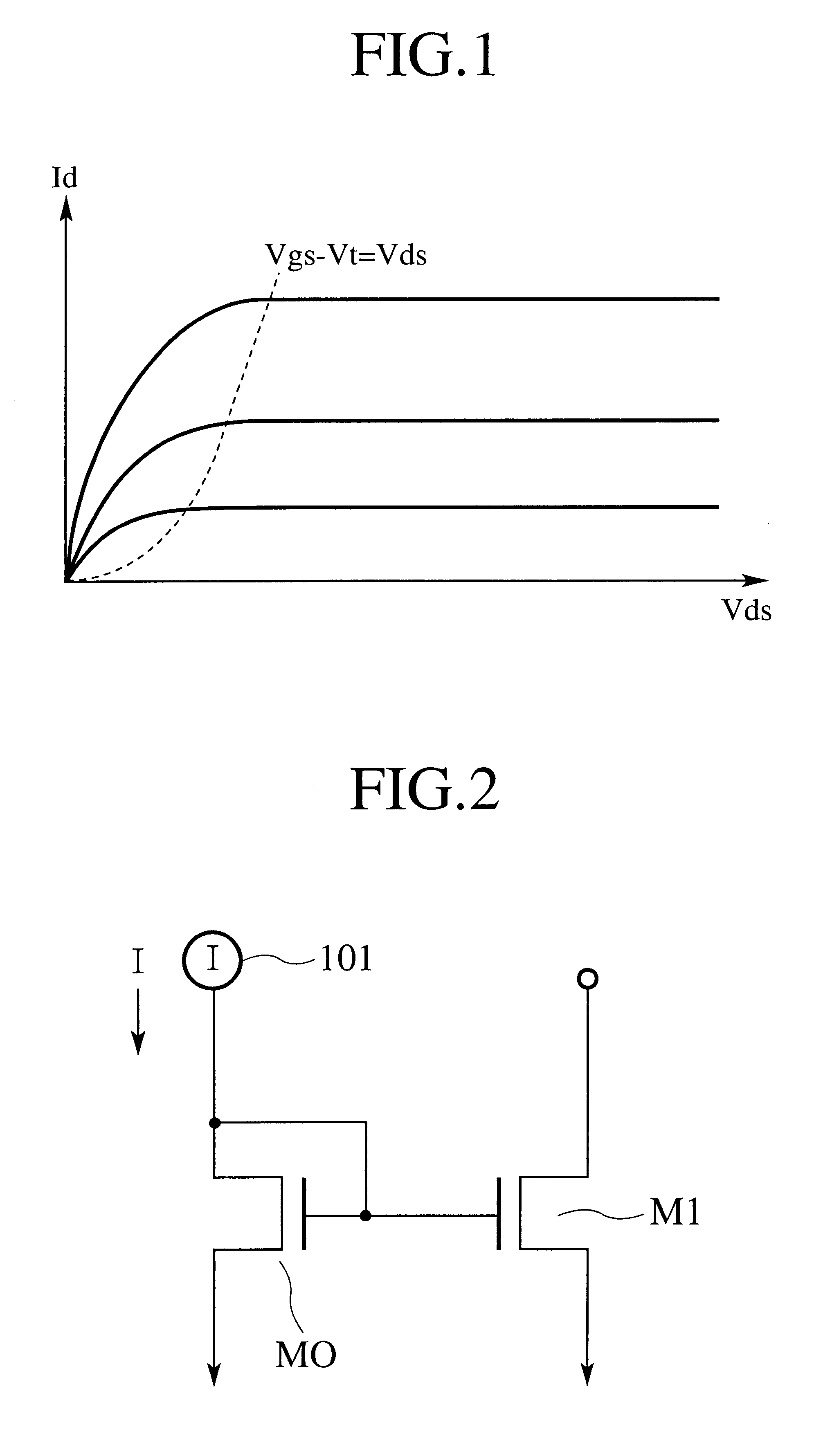
Current mirror circuit and current source circuit
a current source circuit and current mirror technology, applied in the direction of amplifiers, instruments, amplifiers with semiconductor devices/discharge tubes, etc., can solve the problems of inability to obtain accurate current mirroring, excessive manufacturing cost of circuits containing transistors with a lowered threshold voltage, and nmos transistors that barely allow current to flow
- Summary
- Abstract
- Description
- Claims
- Application Information
AI Technical Summary
Problems solved by technology
Method used
Image

Examples
first embodiment
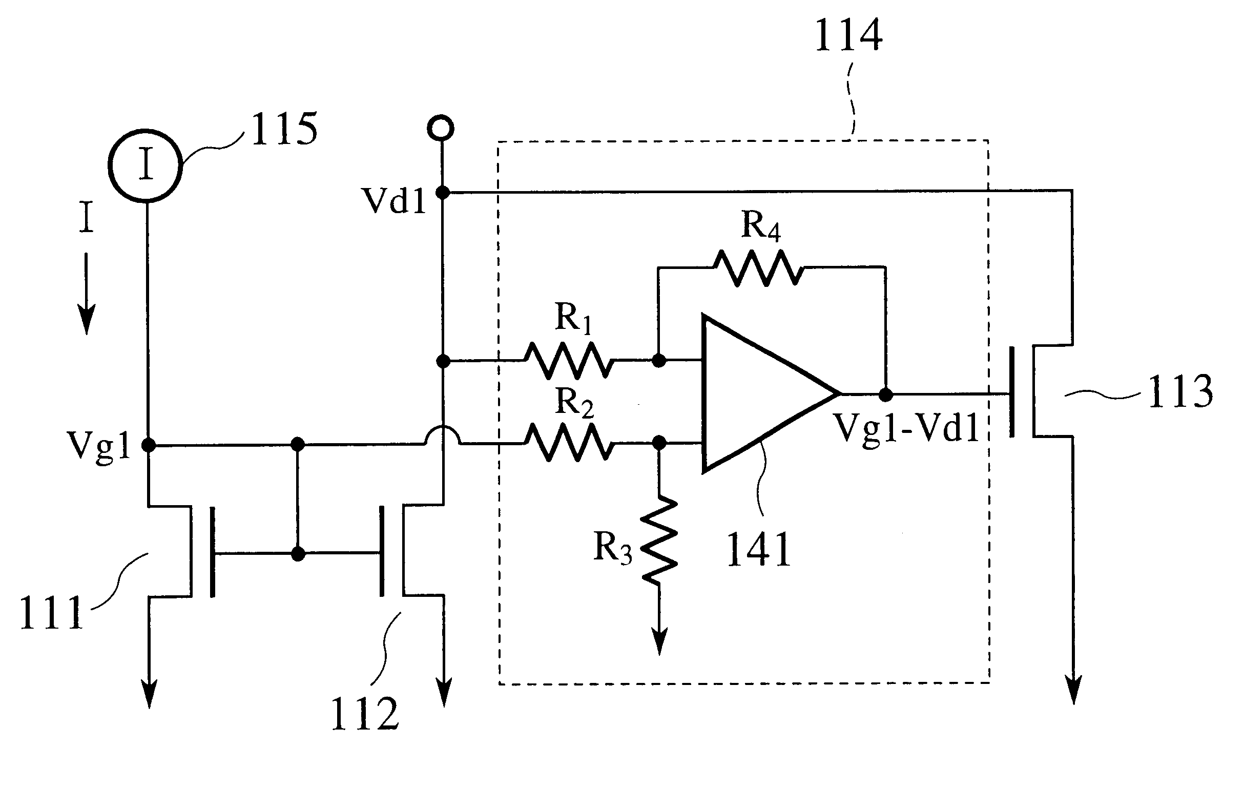
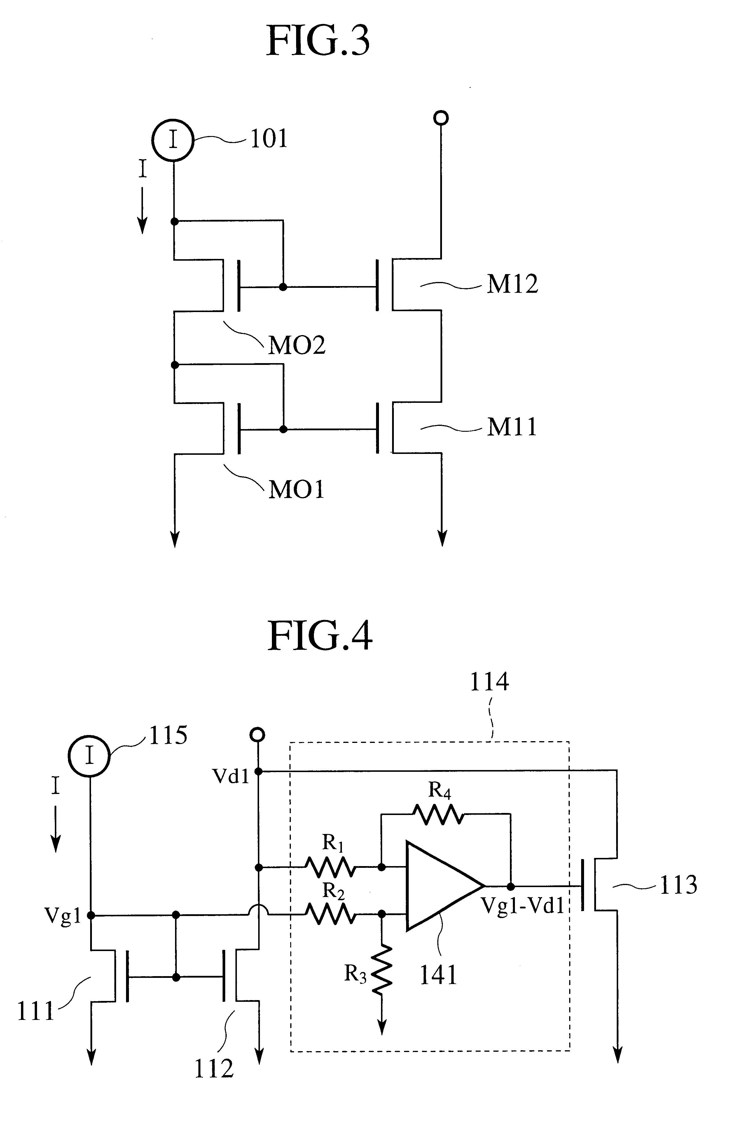
FIG. 4 is a circuit diagram according to a current mirror circuit of the present invention. The current mirror circuit includes NMOS transistors 111 and 112. The current mirror circuit firer includes a compensation circuit to improve the effects of the current mirror circuit. The compensation circuit includes a subtracter 114 and an NMOS transistor 113. The result of the subtracter 114 is input to the gate of NMOS transistor 113. The subtracter 114 is a circuit that outputs the voltage difference between two input signals to the output terminal. The subtracter 114 includes an operational unit 141 and a plurality of resistors R (R.sub.1 -R.sub.4). The voltage V.sub.g1 of the gates of the NMOS transistors 111 and 112, as well as the voltage V.sub.d1 of the drain of the NMOS transistor 112 are input to the subtracter 114, and the subtracter 114 subtracts V.sub.d1 from V.sub.g1. The result (V.sub.g1 -V.sub.d1) is output to the gate of the NMOS transistor 113. In comparison to the on-res...
fifth embodiment
FIG. 9 is a circuit diagram of a current mirror circuit of the present invention. The current mirror circuit includes transistors 111, 112, and a compensation circuit. The compensation circuit includes a PMOS transistor 116 and a level converter 117. Current is supplied to the drain of NMOS transistor 112 through PMOS transistor 116. The bias voltage is applied to the gate-drain of PMOS transistor 116 through the level converter 117.
The gate-drain voltage shown as monotonous decrease function of drain-source voltage is applied to the gate of PMOS transistor 116. Then, the bias voltage applied to the gate of the PMOS transistor 116 comes into decreasing as increasing in the voltage V.sub.d1 of the drain of the NMOS transistor 112. Then the current in the PMOS transistor 116 increase, the current in the NMOS transistor 112 comes into decreasing. Then, though drain-source voltage V.sub.d1 increases, the mirror current is constantly maintained.
Therefore, In this embodiment, adding the P...
seventh embodiment
Therefore, in the seventh embodiment, the drain-source voltage dependency of the mirror current in the pentode region of PMOS transistor 116 can be alleviated.
FIG. 12 is a circuit diagram of an eighth embodiment of a current mirror circuit of the present invention. The eighth embodiment of FIG. 12 uses similar corresponding parts as the eighth embodiment illustrated in FIG. 10, but has been appropriately abbreviated. In the eighth embodiment, PMOS transistors are employed in the circuit. The current mirror circuit includes PMOS transistors 121,122, an NMOS transistor 124, and a level converter 117. The NMOS transistor 124 is connected to the drain of the PMOS transistor 121. The gate of the NMOS transistor 124 is connected to the source of the PMOS transistor 122 through level converter 117 which has monotonous decrease function of the absolute value of the drain-source voltage. When a change occurs in the drain voltage of the PMOS transistor 122, the NMOS transistor 124 causes the ...
PUM
 Abstract
Description
Claims
Application Information