Field-effect semiconductor device, and method of fabrication

a field-effect semiconductor and semiconductor technology, applied in the field of semiconductor devices, can solve the problems of easy triggering into action, inconvenient use of conventional normally-on hemts, and unnecessary complex associated circuitry

Active Publication Date: 2010-06-24
SANKEN ELECTRIC CO LTD
View PDF6 Cites 116 Cited by
  • Summary
  • Abstract
  • Description
  • Claims
  • Application Information

AI Technical Summary

Benefits of technology

[0020]It is among the objects of this invention to render field-effect semiconductor devices of the kind defined, capable of operation in normally-off mode without the difficulties and inconveniences experienced heretofore, while keeping their on-resistance and gate leak current significantly less than in the comparable prior art devices.

Problems solved by technology

Use of such a negative power supply made the associated circuitry unnecessary complex and expensive.
The conventional normally-on HEMTs were rather inconvenient of use.
First, it had a threshold voltage as low as one volt or even less and so was easy to be triggered into action by noise.
What was worse, this threshold changed substantively with manufacturing errors in the depth of the recess in the electron supply layer.
Another weakness was that there was a relatively large current leakage upon application of a positive voltage to the Schottky gate.
Creating the recess in the electron supply layer brought about the additional weakness that the resulting thin part of the electron supply layer was not necessarily satisfactory in its capability of supplying a sufficient amount of electrons to the electron transit layer when a voltage was applied to the gate in order to turn the device on.
The fact that the 2DEG channel was partly insufficient in electron density made the turn-on resistance of the device inordinately high.
The resulting depletion of electrons from under the gate creates a hiatus in the 2DEG layer, making the device normally off.
An objection to this second known suggestion is the difficulty of creating the p-type nitride semiconductor layer of the sufficiently high hole density required.
As an additional disadvantage, the insulating film was susceptible to physical defects, particularly when made thinner for a higher transconductance.
A defective insulating film was a frequent cause of current leakage, lower antivoltage strength, device destruction, and current collapse.
All these results would be avoidable by making the insulating film thicker, but then the device would be inconveniently low in transconductance.
A problem with this prior art device arose when the gate was excited to turn it on.
Similar problems have attended the conventional endeavors to provide other types of normally-off 2DEG diodes and MESFETs and like field-effect semiconductor devices other than HEMTs.

Method used


Image

  • Field-effect semiconductor device, and method of fabrication
  • Field-effect semiconductor device, and method of fabrication
  • Field-effect semiconductor device, and method of fabrication

Examples


embodiment

of FIG. 12

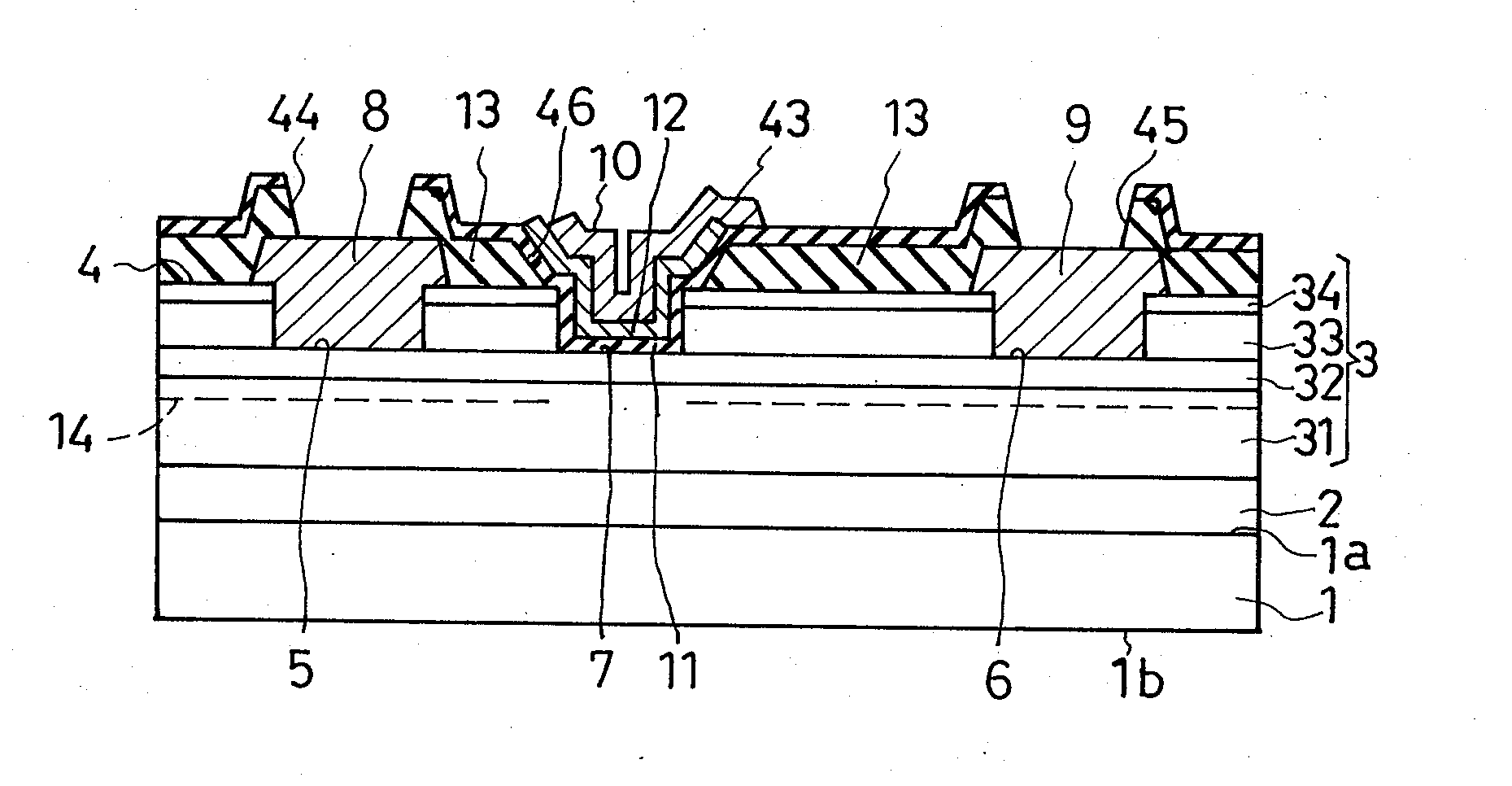
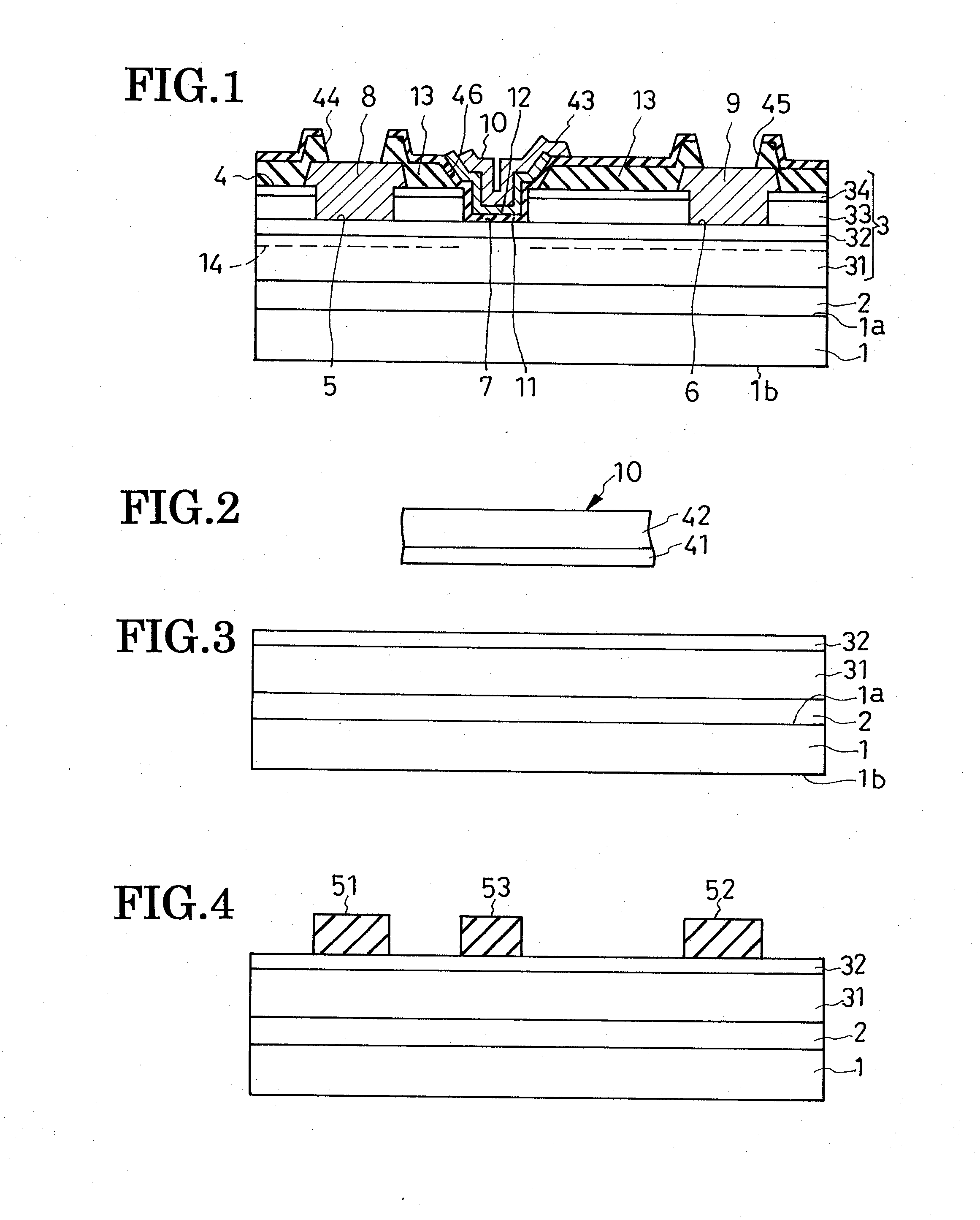
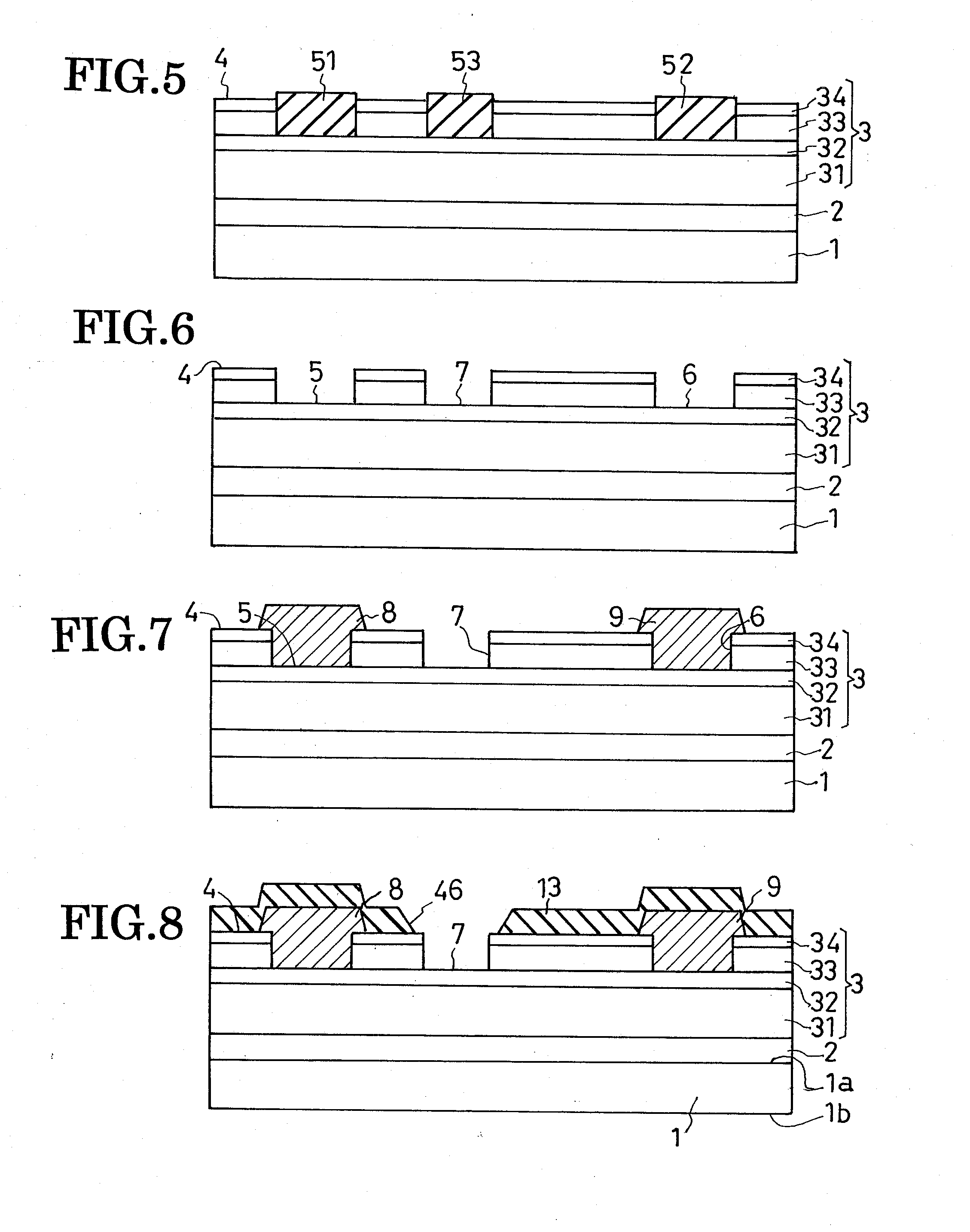
[0121]The second preferred form of heterojunction field-effect semiconductor device according to the invention features a modified insulating film 11a, all the other details of construction being as above described with reference to FIGS. 1 and 2. The modified insulating film 11a differs from its FIG. 1 counterpart 11 in underlying only the p-type metal oxide semiconductor film 12, leaving the protective film 13 exposed. Thus the insulating film 11a is held against the main semiconductor region surfaces defining the third recess 7 and the protective film surfaces bounding the opening 46. Being basically of the same construction as the first disclosed embodiment of the invention, this alternate embodiment offers the same benefits therewith.

Embodiment of FIG. 13

[0122]Another modified insulating film 11b is the sole difference of the device shown in FIG. 13 from that of FIG. 1. The modified insulating film 11b is similar to its FIG. 1 counterpart 11 in underlying the p-type m...


PUM


Abstract

A heterojunction field-effect semiconductor device has a main semiconductor region comprising two layers of dissimilar materials such that a two-dimensional electron gas layer is generated along the heterojunction between the two layers. A source and a drain electrode are placed in spaced positions on a major surface of the main semiconductor region and electrically coupled to the 2DEG layer. Between these electrodes, a gate electrode is received in a recess in the major surface of the main semiconductor region via a p-type metal oxide semiconductor film and insulating film, whereby a depletion zone is normally created in the 2DEG layer, making the device normally off. The p-type metal oxide semiconductor film of high hole concentration serves for the normally-off performance of the device with low gate leak current, and the insulating film for further reduction of gate leak current.

Description

CROSS REFERENCE TO RELATED APPLICATIONS[0001]This application claims priority to Japanese Patent Application No. 2008-328291, filed Dec. 24, 2008.BACKGROUND OF THE INVENTION[0002]This invention relates to semiconductor devices, particularly to field-effect semiconductor devices as typified by the high electron mobility transistor (HEMT), the two-dimensional electron gas (2DEG) diode (diode that utilizes a layer of 2DEG as a current path or channel), and the metal-semiconductor field-effect transistor (MESFET). More particularly, the invention pertains to such field-effect semiconductor devices that are normally off, instead of normally on as in the case of most of such devices known heretofore. The invention also deals with a method of fabricating such normally-off field-effect semiconductor devices.[0003]The HEMT, a type of FET, has been known and used extensively which comprises an electron transit layer overlying a substrate via a buffer, and an electron supply or barrier layer o...

Claims


Application Information

Patent Timeline
Patent Type & Authority Applications(United States)
IPC IPC(8): H01L29/778H01L29/24H01L21/335
CPCH01L29/2003H01L29/66462H01L29/4236H01L29/812H01L29/7786H01L29/4966
Inventor KANEKO, NOBUO
Owner SANKEN ELECTRIC CO LTD
Why Eureka
Try Eureka