Method of forming material using atomic layer deposition and method of forming capacitor of semiconductor device using the same

Inactive Publication Date: 2006-08-08
SAMSUNG ELECTRONICS CO LTD
View PDF7 Cites 44 Cited by
  • Summary
  • Abstract
  • Description
  • Claims
  • Application Information

AI Technical Summary

Benefits of technology

[0021]According to an exemplary embodiment, the present invention involves an ALD process in which a metal alkoxide precursor and an oxidant that contains no hydroxyl group may be reacted to form a thin film having improved step coverage and

Problems solved by technology
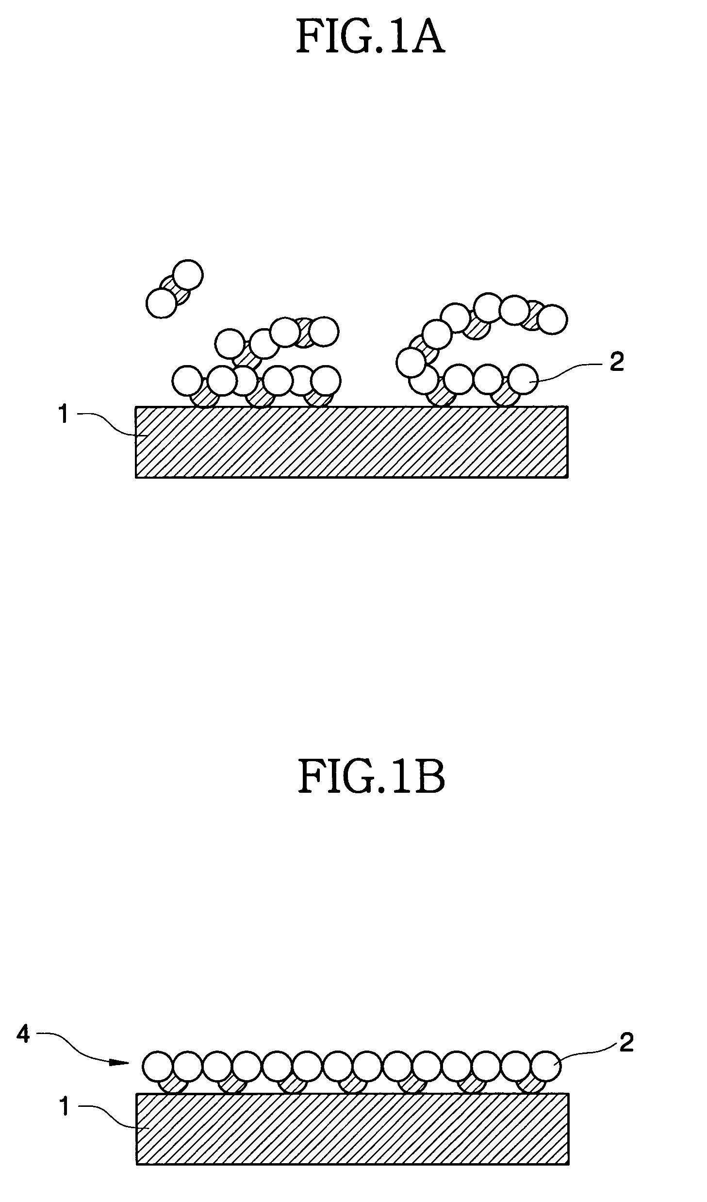
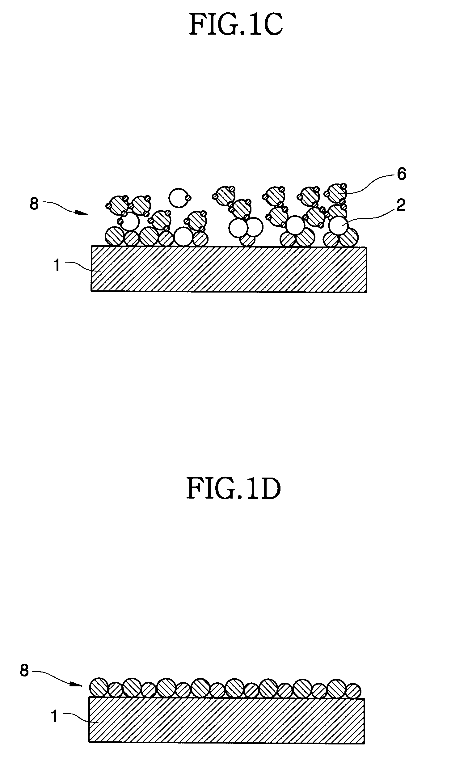
The decrease in cell capacitance resulting from a reduction in available memory cell area makes it difficult to increase the integration density of semiconductor memory devices.
Decreased cell capacitance degrades the data readability from memory cells, increases the soft error rate and also hinders low-voltage operation of the semiconductor memory devices.
However, for memory devices such as dynamic random access memories (DRAMs) having capacities of 1 gigabit or more, it is difficult to obtain sufficient capacitance to ensure satisfactory operation of the memory devices with either of the methods noted above.
However, the use of the Ta2O5 film has a potential problem in that it typically is highly reactive with a polysilicon film.
Further, oxygen vacancies within Ta2O5 film may increase leakage current.
However, the use of a noble metal or a metal nitride presents other potential problems.
Notwithstanding any advantages associated therewith, a composition of these source gases often negatively impacts the coverage of the Ta2O5 film, presumably due to th

Method used


Image

  • Method of forming material using atomic layer deposition and method of forming capacitor of semiconductor device using the same
  • Method of forming material using atomic layer deposition and method of forming capacitor of semiconductor device using the same
  • Method of forming material using atomic layer deposition and method of forming capacitor of semiconductor device using the same

Examples


experiment 1

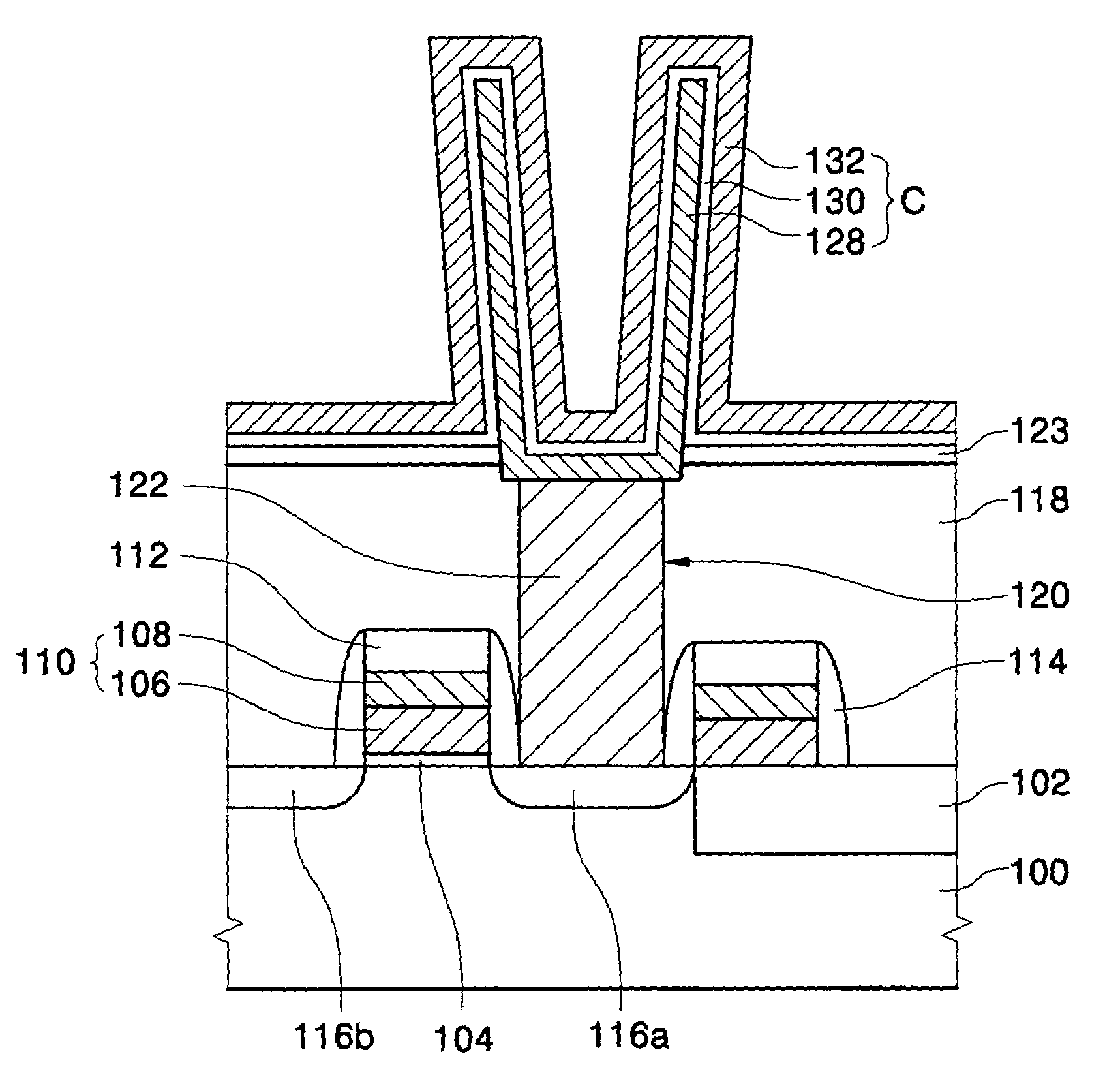
[0093]A tantalum dielectric layer was formed on a cylindrical Ru lower electrode having an aspect ratio of about 15:1 using tetraethoxy tantalum dimethylamino-ethoxide (TAT-DMAE) as a tantalum precursor and O3 gas as an oxygen source. The dielectric layer was formed by an ALD method having a cycle of inflow of tantalum precursors→purging→inflow of O3 gas→purging. In this experiment, the temperature of the chamber was maintained at temperatures of 250° C., 300° C., 350° C. and 400° C. The thickness of the upper portion of a Ta2O5 layer deposited at each temperature (t1 of FIG. 8) and the thickness of the lower portion of the Ta2O5 layer (t2 of FIG. 8) were measured. The results of these measurements are shown below in Table 1.

[0094]

TABLE 1Classification250° C.300° C.350° C.400° C.t1 (Å)240103233244t2 (Å)220102207228

[0095]As shown in Table 1, the thicknesses of the deposited layers vary with temperature. Notwithstanding these differences, it was observed that the Ta2O5 layer exhibited...


PUM

PropertyMeasurementUnit
Temperatureaaaaaaaaaa

Abstract

Disclosed are methods of forming dielectric materials using atomic layer deposition (ALD) and methods of forming dielectric layers from such materials on a semiconductor device. The ALD process utilizes a first reactant containing at least one alkoxide group that is chemisorbed onto a surface of a substrate and then reacted with an activated oxidant that contains no hydroxyl group to form a dielectric material exhibiting excellent step coverage and improved leakage current characteristics.

Description

CROSS-REFERENCE TO RELATED APPLICATIONS[0001]This application is a Continuation-in-part of and claims priority under 35 U.S.C. § 120 to U.S. patent application Ser. No. 10 / 047,706 entitled “SEMICONDUCTOR CAPACITORS HAVING TANTALUM OXIDE LAYERS AND METHODS FOR MANUFACTURING THE SAME”, which was filed on Jan. 15, 2002, now U.S. Pat. No. 6,734,480 the contents of which are herein incorporated by reference in its entirety. This application also claims priority under 35 U.S.C. § 119 from Korean Patent Application Nos. 2001-3165, filed Jan. 19, 2001, and 2002-42217, filed Jul. 18, 2002, the contents of which are also herein incorporated by reference in their entirety.BACKGROUND OF THE INVENTION[0002]1. Field of the Invention[0003]The present invention relates to a method of manufacturing semiconductor devices, and more particularly, to a method of forming a material layer during the manufacture of semiconductor devices using the technique of atomic layer deposition (ALD) and a method of f...

Claims


Application Information

Patent Timeline
IPC IPC(8): H01L21/8242C23C16/40C23C16/44C23C16/455H01L21/316
CPCC23C16/405C23C16/452C23C16/45553H01L21/3141H01L21/31604H01L21/31645H01L21/31691H01L28/40H01L21/31641H01L21/31683H01L21/31637H01L21/02274H01L21/02181H01L21/0228
Inventor YEO, JAE-HYUNKIM, YOUNG-SUNKIM, SUNG-TAEPARK, IN-SUNGIM, GI-VIN
Owner SAMSUNG ELECTRONICS CO LTD
Why Eureka
Try Eureka