Gan semiconductor device

a semiconductor and compound semiconductor technology, applied in semiconductor lasers, semiconductor laser structural details, lasers, etc., can solve the problems of difficult to find a substrate lattice-matched to high density of crystal defects, and grow high-quality gan-based compound semiconductor layers. , to achieve the effect of suppressing current leakage more reliably

Active Publication Date: 2006-05-11
SONY CORP
View PDF5 Cites 46 Cited by
  • Summary
  • Abstract
  • Description
  • Claims
  • Application Information

AI Technical Summary

Benefits of technology

[0061] While the pad metal may be spaced apart from the outer edge of each core portion by a distance of 50 μm or less, the electrode is preferably provided on the multilayer structure

Problems solved by technology

One problem in fabrication of a GaN-based semiconductor light emitting device is that it is difficult to find a substrate lattice-matched to GaN-based compound semiconductor layers.
However, even by providing the low-temperature buffer layer and growing the GaN-based compound semiconductor layers on the low-temperature buffer layer, the density of crystal defects becomes high.
Accordingly, it is difficult to grow high-quality GaN-based compound semiconductor layers, so that it is difficult to fabricate the GaN-based semiconductor light emitting device with high reliability.
However, any other problems associated with the lattice mismatch remain as far as the sapphire substrate is used as the substrate of the GaN-based semiconductor light emitting device.
Further, since the sapphire substrate is dielectric, there is a limit to the arrangement of the electrodes.
However, it is c

Method used


Image

  • Gan semiconductor device
  • Gan semiconductor device
  • Gan semiconductor device

Examples


first preferred embodiment

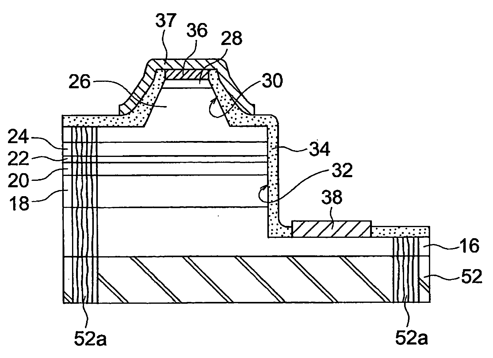
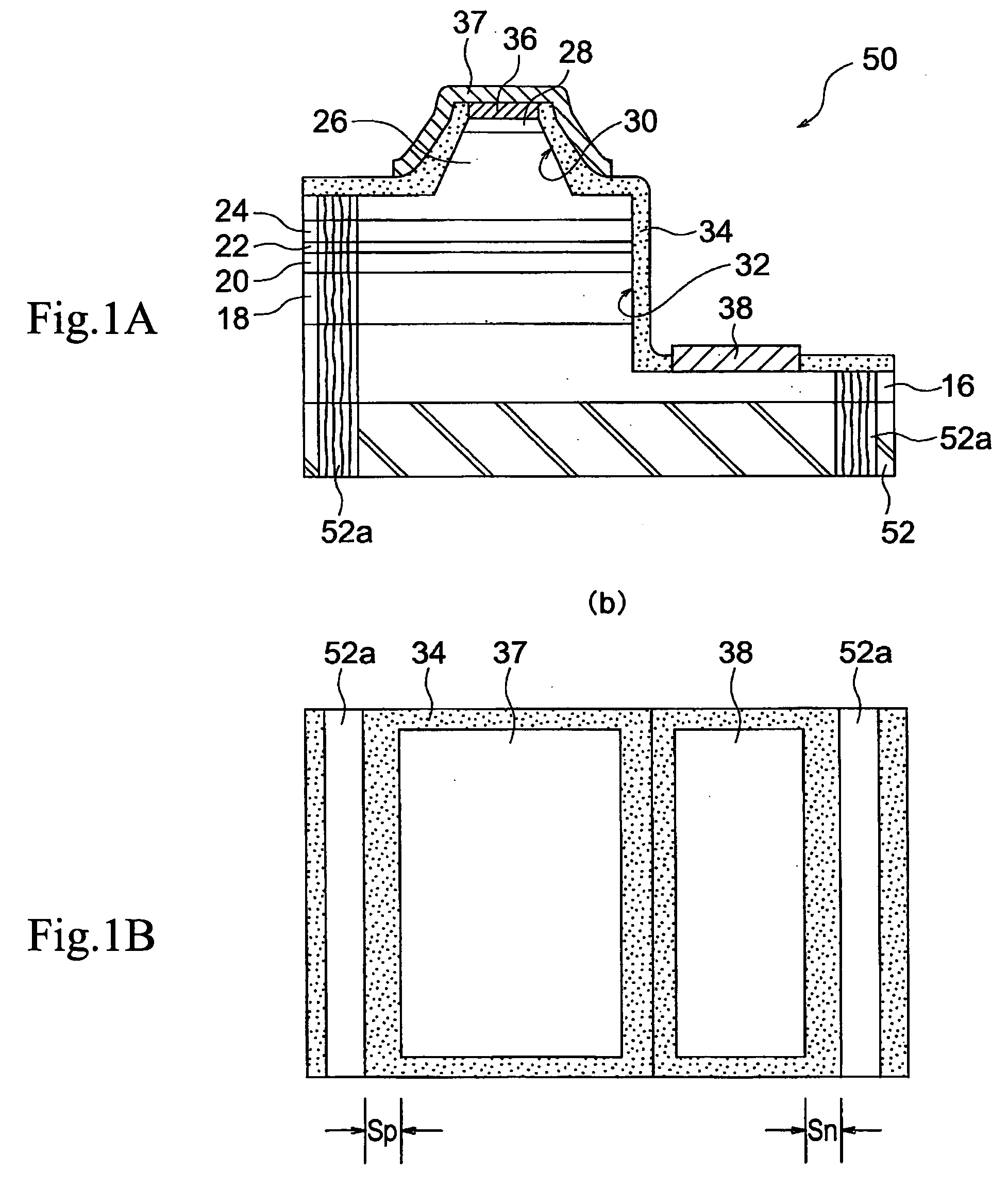
[0082] This preferred embodiment is a preferred embodiment wherein the GaN-based semiconductor device according to the present invention is applied to a GaN-based semiconductor laser device. FIG. 1A is a sectional view showing the configuration of a GaN-based semiconductor laser device according to the first preferred embodiment, and FIG. 1B is a plan view showing the positional relation among a pad metal for a p-side electrode, an n-side electrode, and core portions in the GaN-based semiconductor laser device shown in FIG. 1A.

[0083] The GaN-based semiconductor laser device 50 is a semiconductor laser device having a structure such that both the p-side electrode and the n-side electrode are provided on the multilayer structure for the convenience of mounting of the semiconductor laser device. As shown in FIG. 1A, the GaN-based semiconductor laser device 50 is similar in configuration to the GaN-based semiconductor laser device 10 shown in FIG. 5 except that a novel GaN substrate 52...

second preferred embodiment

[0102] This preferred embodiment is another preferred embodiment wherein the GaN-based semiconductor device according to the present invention is applied to a GaN-based semiconductor laser device. FIG. 4A is a sectional view showing the configuration of a GaN-based semiconductor laser device according to the second preferred embodiment, and FIG. 4B is a plan view showing the positional relation among a pad metal for a p-side electrode, an n-side electrode, and core portions in the GaN-based semiconductor laser device.

[0103] The GaN-based semiconductor laser device 60 is a semiconductor laser device having a structure such that the p-side electrode is provided on the multilayer structure, and the n-side electrode is provided on the back surface of the substrate. As shown in FIG. 4A, the GaN-based semiconductor laser device 60 is similar in configuration to the GaN-based semiconductor laser device 10 shown in FIG. 5 except that a novel GaN substrate 62 having the above-mentioned char...


PUM


Abstract

Provided is a GaN-based semiconductor light emitting device formed on a GaN single-crystal substrate and having a configuration capable of reducing a current leak.
A GaN-based semiconductor laser device (50) is disclosed as an example of the GaN-based semiconductor light emitting device, and it is a semiconductor laser device having a structure such that a p-side electrode and an n-side electrode are provided on a multilayer structure of GaN-based compound semiconductor layers. The GaN-based semiconductor laser device (50) is similar in configuration to a conventional GaN-based semiconductor laser device formed on a sapphire substrate except that a GaN single-crystal substrate (52) is used in place of the sapphire substrate and that the multilayer structure is directly formed on the GaN single-crystal substrate (52) without providing a GaN-ELO structure layer. The GaN single-crystal substrate (52) has continuous belt-shaped core portions (52a) each having a width of 10 μm. These core portions (52a) are spaced apart from each other by a distance of about 400 μm. A laser stripe (30), a pad metal (37) for the p-side electrode (36), and the n-side electrode (38) are provided on the multilayer structure in a region except the core portions (52a) of the GaN single-crystal substrate (52). The horizontal distance Sp between the pad metal (37) and the core portion (52a) adjacent thereto is 95 μm, and the horizontal distance Sn between the n-side electrode (38) and the core portion (52a) adjacent thereto is also 95 μm.

Description

TECHNICAL FIELD [0001] The present invention relates to a GaN-based semiconductor device, and more particularly to a GaN-based semiconductor device which can reduce a current leak. Further, the invention relates to a GaN-based semiconductor light emitting device which can reduce a current leak to improve a light emission efficiency. BACKGROUND ART [0002] A III-V gallium nitride (GaN)-based compound semiconductor such as GaN, GaInN, and AlGaInN has a wide bandgap of 2.8 to 6.8 eV, and attention is focused on such a GaN-based compound semiconductor as the material of a semiconductor light emitting device capable of emitting light in a red to UV region. [0003] As a GaN-based semiconductor light emitting device using a III-V GaN-based compound semiconductor as a component, a blue or green light emitting diode (LED) and a GaN-based semiconductor laser device oscillating in a violet region of about 405 nm, for example, have been developed and put into practical use. [0004] One problem in ...

Claims


Application Information

Patent Timeline
IPC IPC(8): H01L33/00H01L33/06H01L33/14H01L33/32H01L33/36H01L33/44H01S5/02H01S5/323H01S5/343
CPCH01S5/0014H01S5/0207H01S5/32341H01S5/2201H01S5/0422
Inventor GOTO, OSAMUMATSUMOTO, OSAMUSASAKI, TOMOMIIKEDA, MASAO
Owner SONY CORP
Why Eureka
Try Eureka