Solid state imaging device capable of parallel reading of data from a plurality of pixel cells

Active Publication Date: 2009-11-26
PANASONIC SEMICON SOLUTIONS CO LTD
View PDF6 Cites 12 Cited by
  • Summary
  • Abstract
  • Description
  • Claims
  • Application Information

AI Technical Summary

Benefits of technology

[0029]With the above-described optional structure, the second conductive layer is disposed between the charge storage portion of the second pixel cell and the first output signal line. Similarly to the above-mentioned conductive layer disposed between the charge storage portion of the first pixel cell and the second output signal line, the second conductive layer serves to suppress the capacitive coupling between the charge storage porti

Problems solved by technology

However, the conventional MOS-type solid state imaging device described above involves the following problem.
As described abov

Method used


Image

  • Solid state imaging device capable of parallel reading of data from a plurality of pixel cells
  • Solid state imaging device capable of parallel reading of data from a plurality of pixel cells
  • Solid state imaging device capable of parallel reading of data from a plurality of pixel cells

Examples


Example

Embodiment 1

1. Overall Structure

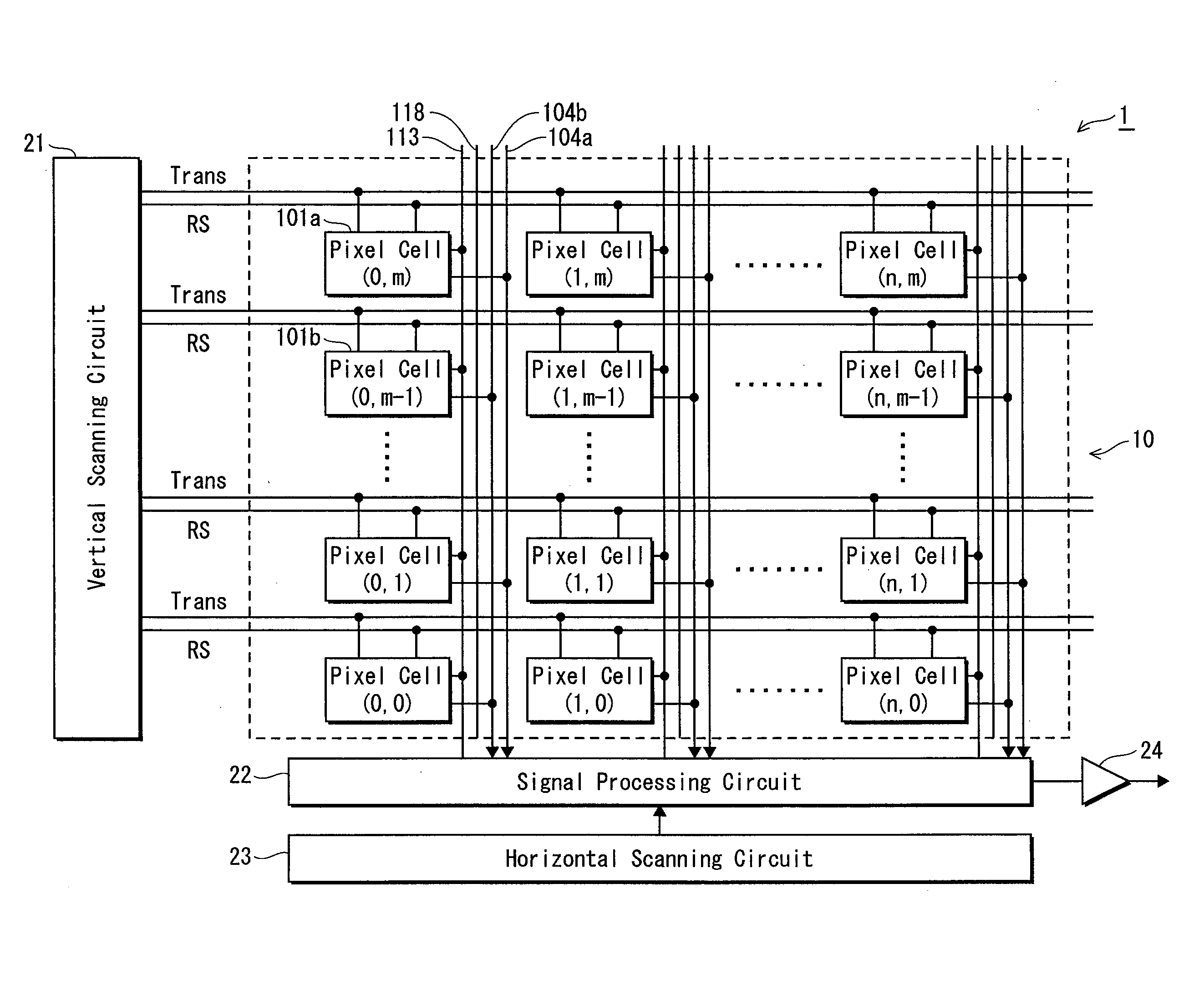
[0059]The following describes the overall structure of a solid state imaging device 1 according to Embodiment 1 of the present invention, with reference to FIG. 3.

[0060]As shown in FIG. 3, the MOS-type solid state imaging device 1 has a pixel region 10 and a circuit region. The pixel region 10 is composed of a plurality of pixel cells 101a and 101b. The circuit region is composed of various circuits, including a vertical scanning circuit 21, a signal processing circuit 22, a horizontal scanning circuit 23, and an amplifier circuit 24.

[0061]In the pixel region 10, the plurality of pixel cells 101a and 101b are arranged in an array, which is one example of a two-dimensional arrangement. The array consists of (n+1) pixel cells per row and (m+1) pixels per column. In the pixel region 10, a transfer control signal line Trans and a reset signal line RS are provided for each row. In addition, a pair of output signal lines 104a and 104b, a pixel selecting lin...

Example

Embodiment 2

[0091]The following describes the structure of a MOS-type solid state imaging device according to Embodiment 2, with reference to FIGS. 12-18.

1. Layout of Pixel Cells 301a and 301b

[0092]The following describes the layout of pixel cells 301a and 301b of the MOS-type solid state imaging device according to Embodiment 2, with reference to FIGS. 12-14.

[0093]Since the layout of Embodiment 1 shown in FIG. 5 is commonly applicable to the MOS-type solid state imaging device according to Embodiment 2, no further illustration and description thereof is given here.

[0094]Similarly to the MOS-type solid state imaging device according to Modification 1 (see FIG. 10) and as shown in FIG. 12, the MOS-type solid state imaging device according to Embodiment 2 has dummy lines 315 each disposed to extend in the Y direction in parallel to the pixel selecting lines 113 in a manner that first layers 304a1 and 304b1 of the output signal lines as well as the charge storage portions 109a and 109...

Example

Embodiment 3

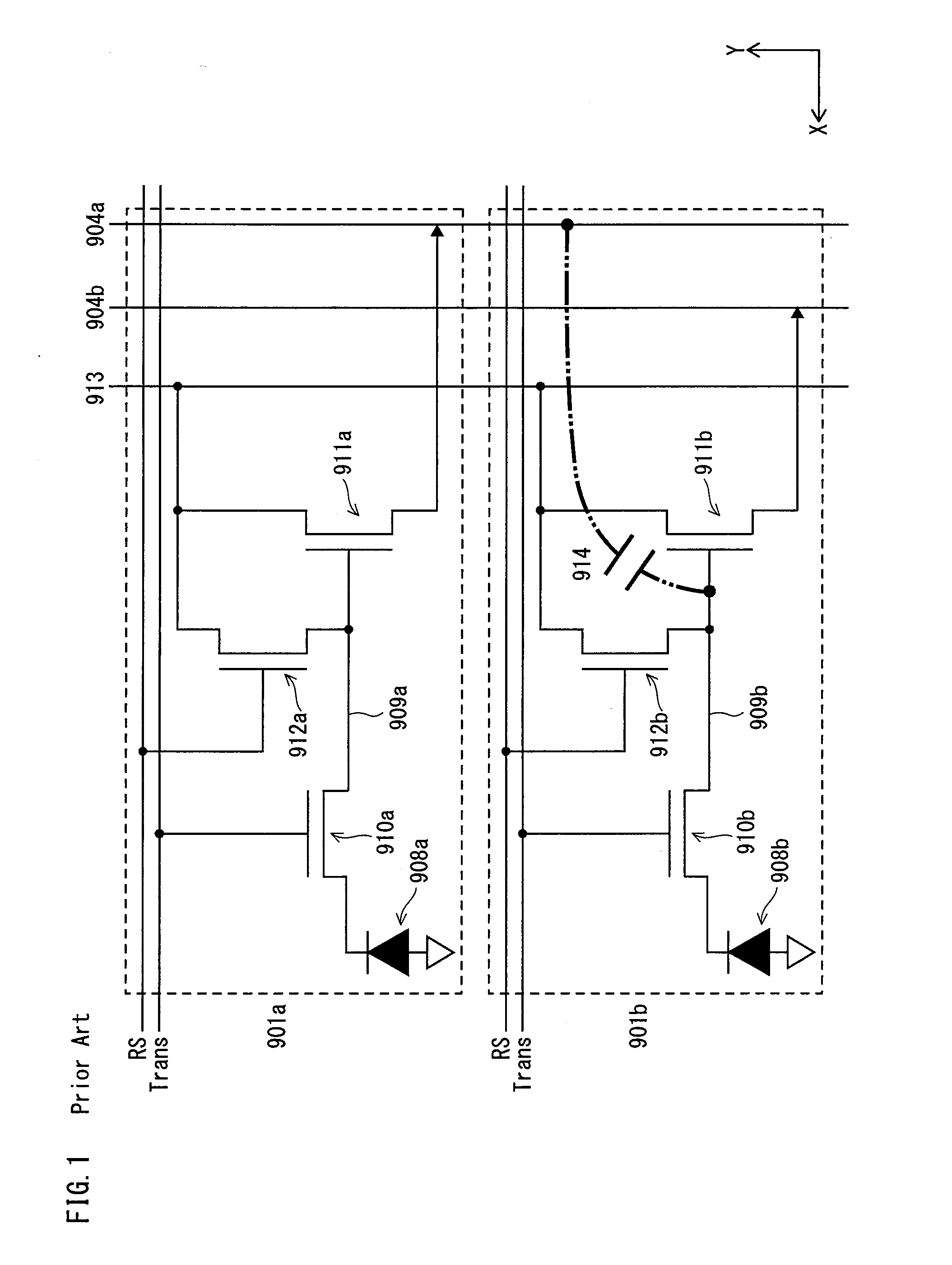
[0118]The following describes the structure of a MOS-type solid state imaging device according to Embodiment 3, with reference to FIG. 20A. Note that the pixel cells 101a and 101b are respectively identical in structure to the pixel cells 101a and 101b of the MOS-type solid state imaging device according to Embodiment 1. In addition, the output signal lines 104a and 104b and other components are identical in structure to the corresponding components described above. Thus, those identical or similar components are not shown in the figures.

[0119]As shown in FIG. 20A, the MOS-type solid state imaging device according to Embodiment 3 has such an imaging region in which the pixel cells 101a and the pixel cells 101b are alternately disposed in the Y direction. In the X direction, on the other hand, each pixel cell 101a is adjacent to another pixel cell 101a, and each pixel cell 101b is adjacent to another pixel cell 101b.

[0120]With the above described arrangement of the pixel...


PUM


Abstract

A solid state imaging device has a pixel region composed of a matrix of pixel cells each including a photodiode and a charge storage portion. First and second output signal lines are in parallel and adjacent to both the charge storage portions of a first pixel cell and a second pixel cells that are adjacent on a same column. A signal voltage of a signal charge in the charge storage portion of the first pixel cell is output to the first output signal line, whereas a signal voltage of a signal charge in the charge storage portion of the second pixel cell is output to the second output signal line. The respective outputs to the first and second output signal lines are processed in parallel. A conductive layer is disposed between the charge storage portion of the first pixel cell and the second output signal line to suppress capacitive coupling.

Description

BACKGROUND OF THE INVENTION[0001](1) Field of the Invention[0002]The present invention relates to a solid state imaging device capable of parallel reading of data from a plurality of pixel cells, and especially to a technique for suppressing occurrences of crosstalk.[0003](2) Description of the Related Art[0004]Solid state imaging devices have been commonly used as image capturing devices such as digital still cameras. One type of solid state imaging device is a MOS-type solid state imaging device having a sensor unit composed of a plurality of pixel cells arranged two-dimensionally (in an array, for example). In order to provide digital still cameras with additional values, such as continuous shooting capability and video shooting capability, it is desirable to improve MOS-type solid state imaging devices in the data readout rate (i.e., the speed at which data is read) from the sensor unit as much as possible.[0005]Various suggestions have been made to improve MOS-type solid state ...

Claims


Application Information

Patent Timeline
IPC IPC(8): H04N5/335H01L27/146H04N5/341H04N5/357H04N5/369H04N5/374
CPCH01L27/14603H04N5/3745H04N5/357H01L27/14636H04N25/60H04N25/77
Inventor OHTSUKI, HIROHISA
Owner PANASONIC SEMICON SOLUTIONS CO LTD
Why Eureka
Try Eureka