Optical chip module and optical chip module device

Inactive Publication Date: 2006-04-18
SHINKO ELECTRIC IND CO LTD
View PDF5 Cites 3 Cited by
  • Summary
  • Abstract
  • Description
  • Claims
  • Application Information

AI Technical Summary

Benefits of technology

[0007]An object of the present invention is to provide a optical chip module enabling direct connection of the optical chip and optical fiber, facilitating positioning of the optical chip and optical fiber, enabling suppression of optical coupling loss, and enabling easy mounting on a board for formation of a module device and an optical chip module device using this optical chip module.

Problems solved by technology

There was the problem that it was necessary to arrange the element forming face of the optical chip 10 and the end face of the optical fiber 20 away from each other.

Method used


Image

  • Optical chip module and optical chip module device
  • Optical chip module and optical chip module device
  • Optical chip module and optical chip module device

Examples


Embodiment Construction

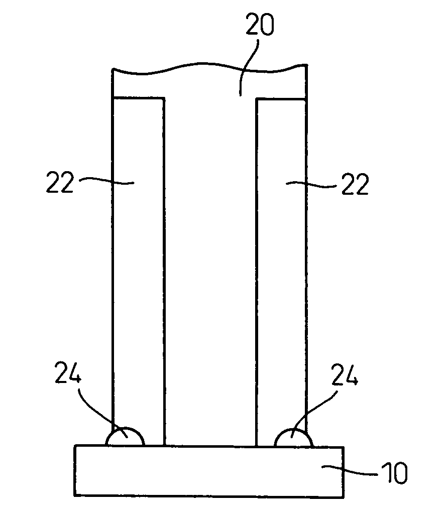
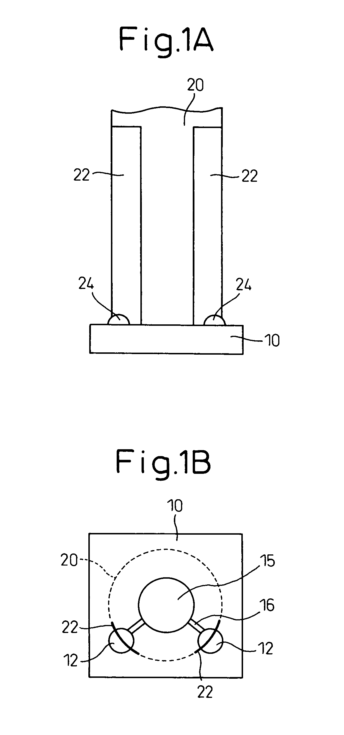
[0019]Preferred embodiments of the present invention will be described in detail below while referring to the attached figures. FIGS. 1A and 1B are views explaining the configuration of an optical chip module according to the present invention. FIG. 1A shows the shape of an optical chip module comprised of an optical chip 10 and an optical fiber 20 as seen from the side direction, while FIG. 1B shows the planar arrangement at an element forming face of the optical chip 10. As shown in FIG. 1A, the optical chip module according to the present invention is comprised of an optical chip 10 on the element forming face of which an end face of an optical fiber 20 is made to abut and the optical chip 10 and optical fiber 20 bonded in that state.

[0020]As shown in FIG. 1B, the element forming face of the optical chip 10 is formed with an element part 15 serving as a light emitting part or light receiving part and terminals electrically connected with the element part 15 through interconnect p...


PUM


Abstract

An optical chip module has an optical chip on an element forming face with a light emitting or a light receiving element and terminals for electrical connection with the element and an optical fiber optically bonded to the element with its end face abutting the element. The outer circumference of the optical fiber has interconnect patterns extending from the end face, and in the axial direction, of the optical fiber and electrically connected with the terminals. Terminals of the optical chip are connected with the interconnect patterns at the end face of the optical fiber, intersecting circumferential lines of the end face of the optical fiber abutting against the element forming face and bonded thereto.

Description

BACKGROUND OF THE INVENTION[0001]1. Field of the Invention[0002]The present invention relates to an optical chip module comprised of a combination of a planar light emitting laser diode or photodiode or other optical chip for emitting light or receiving light and an optical fiber and to an optical chip module device comprised of this optical chip module mounted on a board.[0003]2. Description of the Related Art[0004]An optical chip module using a planar light emitting laser diode or photo diode or other optical chip for emitting light or receiving light, as shown in FIG. 6, has an optical fiber 20 arranged so that its end face faces the light emitting face or light receiving face of the optical chip 10 and projects or receives light between the optical chip 10 and optical fiber 20. In FIG. 6, 12 indicates terminals of the optical chip 10, 13 bonding wires bonded to the terminal 12, and 14 connection electrodes of the mounting board. Further, FIG. 7 shows an element forming face of t...

Claims


Application Information

Patent Timeline
IPC IPC(8): G02B6/42G02B6/12G02B6/30H01L31/0232H01S5/022
CPCG02B6/4228G02B6/4238G02B6/423
Inventor IWAI, JUNICHI
Owner SHINKO ELECTRIC IND CO LTD
Why Eureka
Try Eureka