Solid-state image pickup device, driving method for solid-state image pickup device, and image pickup apparatus

a driving method and image technology, applied in the direction of radio frequency controlled devices, television system scanning details, television systems, etc., can solve the problems of increased power consumption and noise for simultaneous resetting, difficult control circuit configuration,

Inactive Publication Date: 2006-10-26
SONY SEMICON SOLUTIONS CORP
View PDF7 Cites 17 Cited by
  • Summary
  • Abstract
  • Description
  • Claims
  • Application Information

AI Technical Summary

Benefits of technology

[0016] Thus, it is desirable to provide a solid-state image pickup device that is capable of reliably suppressing occurrence of blooming irrespective of setting of a partial-read region, a driving method for the solid-state image pickup device, and an image pickup apparatus.
[0018] Since the solid-state image pickup device having the above-mentioned structure sequentially resets pixels in the particular regions row by row when the signals of the pixels in the desired region are sequentially read row by row, electric charges stored in a photoelectric conversion element in each pixel in the particular regions does not exceed the storage capacity of the photoelectric conversion element without performing a reading operation for a region other than the desired region. Thus, electric charges stored in the photoelectric conversion element in each pixel in the particular regions are less likely to exceed the storage capacity of the photoelectric conversion element and less likely to leak to peripheral pixels, that is, to pixels in a desired partial-read region.
[0019] Accordingly, occurrence of blooming can be reliably suppressed, irrespective of setting of the desired region.

Problems solved by technology

In this case, however, it is difficult to configure a control circuit for performing reset control on all the non-access rows other than the desired partial-read region 104 while setting the partial-read region 104.
In addition, there is a concern about increases in power consumption and noise for simultaneous resetting.

Method used


Image

  • Solid-state image pickup device, driving method for solid-state image pickup device, and image pickup apparatus
  • Solid-state image pickup device, driving method for solid-state image pickup device, and image pickup apparatus
  • Solid-state image pickup device, driving method for solid-state image pickup device, and image pickup apparatus

Examples


first embodiment

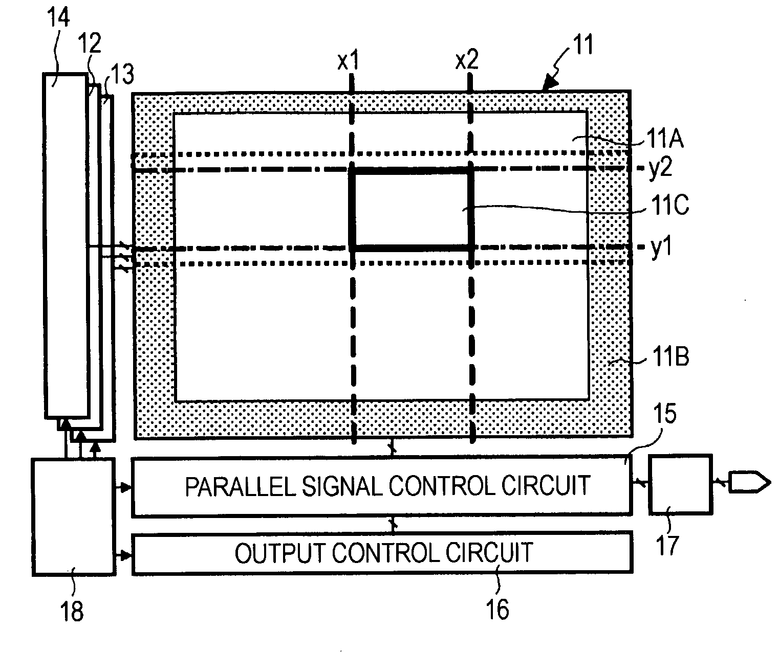
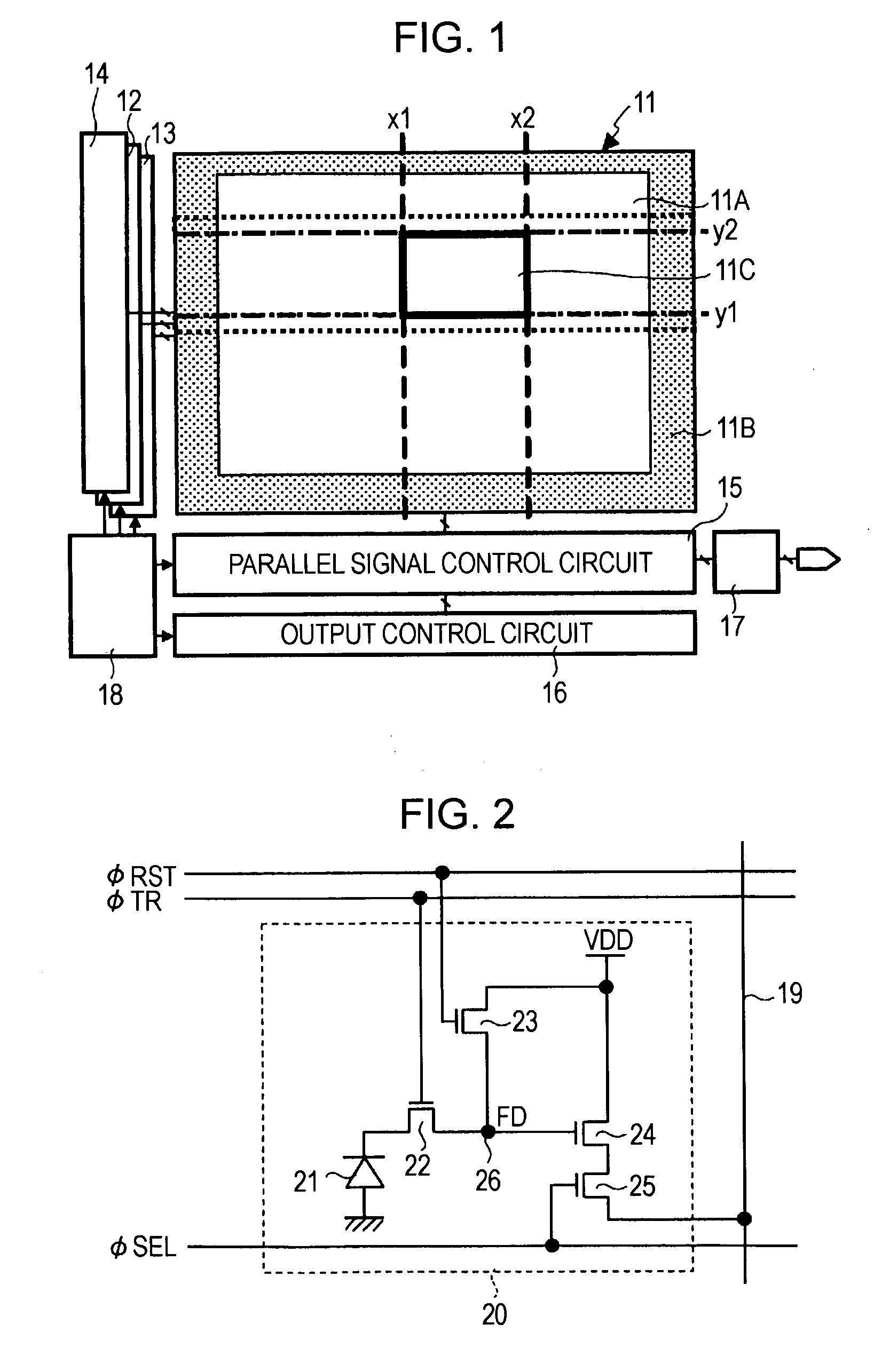
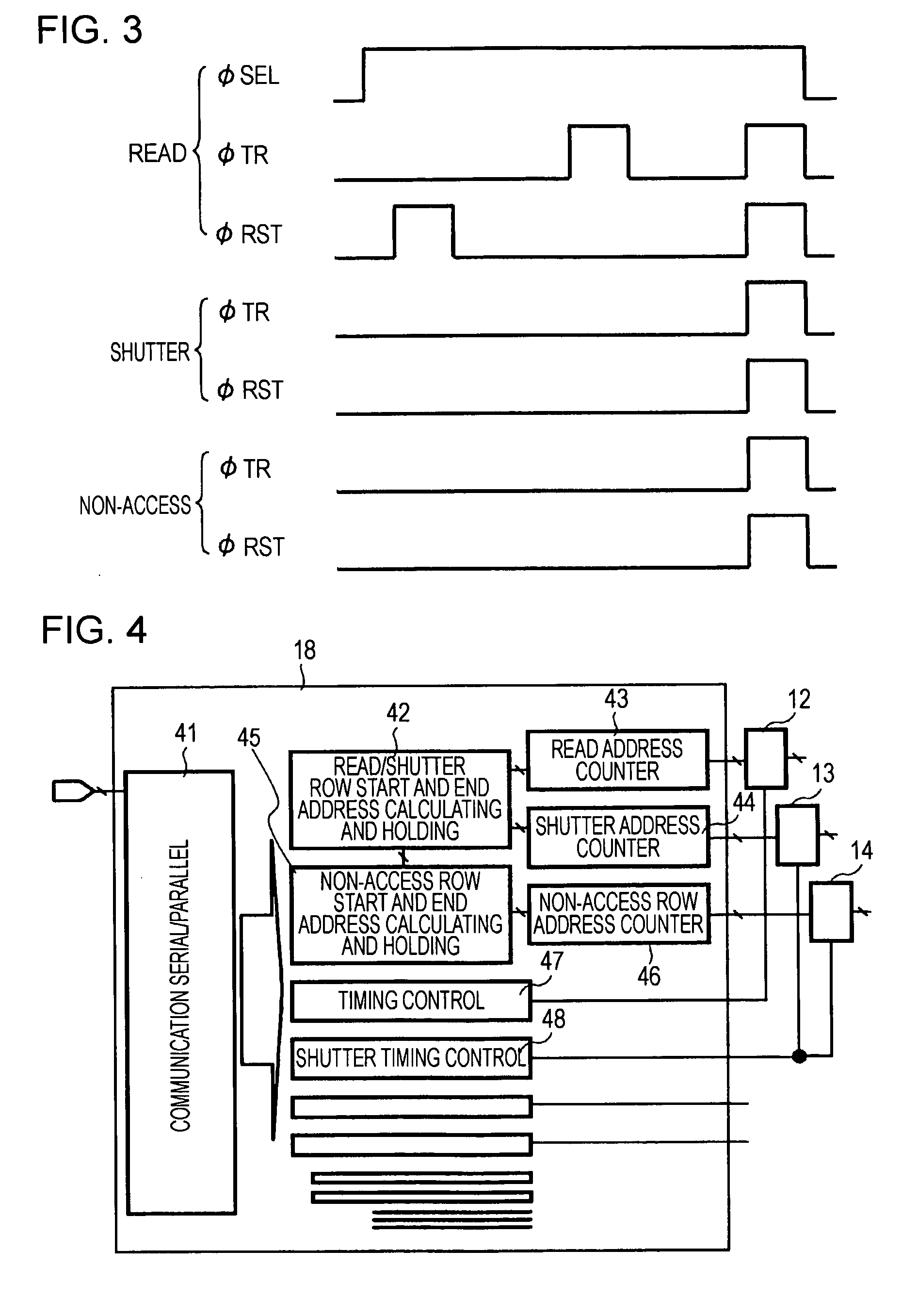
[0034]FIG. 1 is a block diagram schematically showing the structure of an X-Y-address-type solid-state image pickup device, such as a CMOS image sensor, according to a first embodiment of the present invention.

[0035] Referring to FIG. 1, a CMOS image sensor according the first embodiment includes a pixel array area 11 in which pixels (not shown) each including a photoelectric conversion element are two-dimensionally arranged. The CMOS image sensor also includes a row read control circuit 12, a row reset control circuit 13, a non-access row reset control circuit 14, a parallel signal processing circuit 15, an output control circuit 16, an amplifying circuit 17, and a timing control circuit 18, which are peripheral circuits of the pixel array area 11. These peripheral circuits are formed, for example, on the same chip (semiconductor substrate) as the pixel array area 11.

[0036] The pixel array area 11 includes an effective pixel region 11A, a light-shielded pixel region 11B, and a pa...

first modification

[0074]FIG. 6 is a schematic diagram showing the pixel array area 11 in a CMOS image sensor according to a first modification of the present invention. In FIG. 6, the equivalent parts as in FIG. 1 are referred to with the same reference numerals.

[0075] In the first modification, although the basic structure and operation are similar to those in the first embodiment, a feature of the first modification is that pixel information in ranges 11F and 11G (the ranges encircled by thick lines in FIG. 6) of the light-shielded pixel region 11B, as well as pixel information in the partial-read region 11C, is read when partial reading is performed.

[0076] In this case, for the non-access row reset regions 11D and 11E, operations and advantages provided by resetting can be achieved, as in the first embodiment. In addition, reading pixel information in the light-shielded pixel region 11B facilitates black level setting.

[0077] In the first modification, when the light-shielded pixel region 11B is...

second modification

[0079]FIG. 7 is a schematic diagram showing the pixel array area 11 in a CMOS image sensor according to a second modification of the present invention. In FIG. 7, the equivalent parts as in FIG. 1 are referred to with the same reference numerals.

[0080] In the first embodiment, the number of rows of the non-access row reset regions 11D and 11E can be set in accordance with an externally set value. However, in the second modification, instead of externally setting the number of rows of the non-access row reset regions 11D and 11E, the number of rows of each of the non-access row reset regions 11D and 11E below and above the partial-read region 11C is fixedly set to half the number of rows of the partial-read region 11C.

[0081]FIG. 8 is a block diagram showing an example of the structure of a non-access row start and end address calculating and holding block 45′ in the second modification. In FIG. 8, the equivalent parts as in FIG. 5 are referred to with the same reference numerals.

[...


PUM


Abstract

A solid-state image pickup device includes a pixel array area in which pixels each including a photoelectric conversion element are two-dimensionally arranged; first control means for performing control such that signals of pixels in a desired region of the pixel array area are sequentially read row by row; and second control means for performing control such that, when the signals of the pixels in the desired region are sequentially read row by row by the first control means, pixels in particular regions below and above the desired region are sequentially reset row by row.

Description

CROSS REFERENCES TO RELATED APPLICATIONS [0001] The present invention contains subject matter related to Japanese Patent Application JP 2005-127628 filed in the Japanese Patent Office on Apr. 26, 2005, the entire contents of which are incorporated herein by reference. BACKGROUND OF THE INVENTION [0002] 1. Field of the Invention [0003] The present invention relates to solid-state image pickup devices, driving methods for solid-state image pickup devices, and image pickup apparatuses, and more particularly, to an X-Y-address-type solid-state image pickup device that includes a pixel array area in which pixels each including a photoelectric conversion element are two-dimensionally arranged and that is capable of segmenting and reading pixel information in a desired region of the pixel array area, to a driving method for the solid-state image pickup device, and to an image pickup apparatus using the solid-state image pickup device as an image pickup device. [0004] 2. Description of the ...

Claims


Application Information

Patent Timeline
Patent Type & Authority Applications(United States)
IPC IPC(8): H01L29/04H04N5/335H04N5/353H04N5/359H04N5/369H04N5/374H04N5/376
CPCH04N3/1562H04N25/443H04N25/63H04N25/745H04N25/76
Inventor MURAMATSU, YOSHINORIABIRU, TAKAHIROHIRATA, TAKAICHI
Owner SONY SEMICON SOLUTIONS CORP
Why Eureka
Try Eureka