Solid-state imaging device and manufacturing method of the same, and electronic apparatus

a technology of solid-state imaging and manufacturing methods, applied in semiconductor devices, diodes, radiation controlled devices, etc., can solve problems such as difficulty in suppressing color mixing, and achieve the effect of reliably suppressing the occurrence of color mixing

Active Publication Date: 2015-01-29
SONY CORP
View PDF1 Cites 15 Cited by
  • Summary
  • Abstract
  • Description
  • Claims
  • Application Information

AI Technical Summary

Benefits of technology

[0016]According to the aspects of the present disclosure, it is possible to more reliably suppress occurrence of color mixing.

Problems solved by technology

Accordingly, in a fine pixel, since an electric field in the transverse direction in the vicinity of the back surface of the device substrate is weak, it is difficult to suppress the color mixing due to the leakage of electrons generated by the photoelectric conversion to adjacent pixels.

Method used


Image

  • Solid-state imaging device and manufacturing method of the same, and electronic apparatus
  • Solid-state imaging device and manufacturing method of the same, and electronic apparatus
  • Solid-state imaging device and manufacturing method of the same, and electronic apparatus

Examples


Embodiment Construction

[0031]Hereinafter, specific embodiments to which the present technology is applied will be described in detail with reference to drawings.

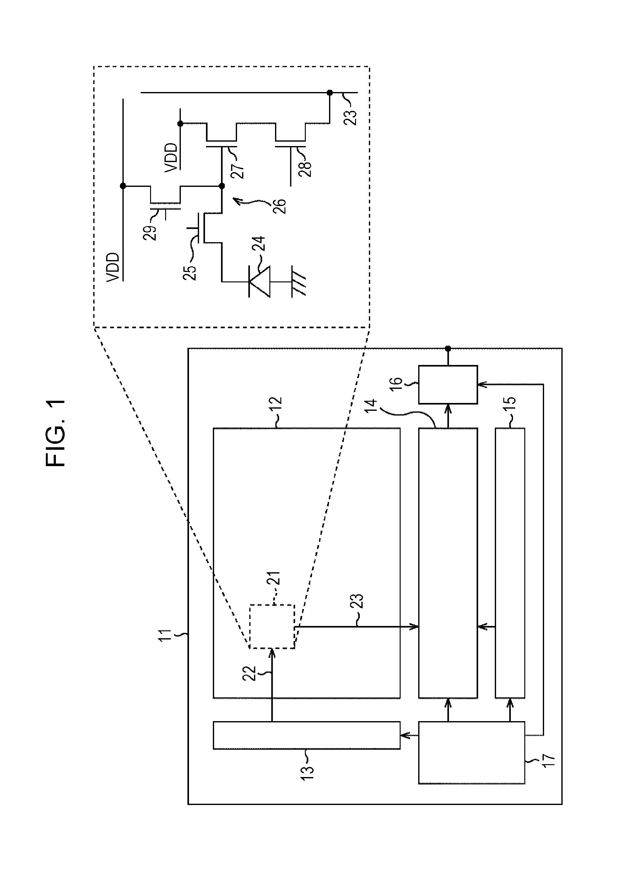
[0032]FIG. 1 is a block diagram illustrating a configuration example of an imaging device to which an embodiment of the present technology is applied.

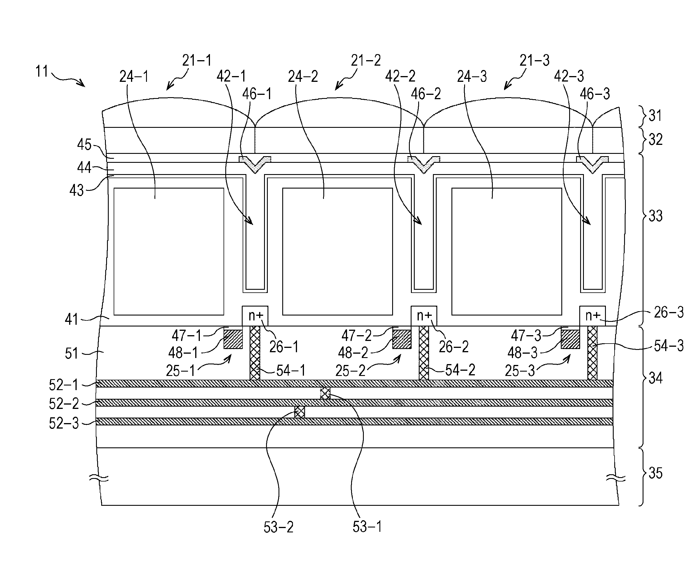
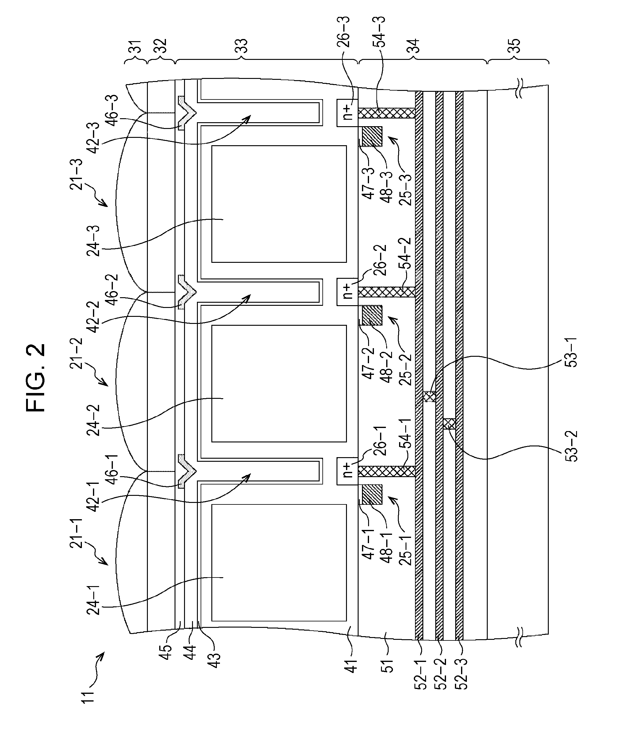
[0033]As illustrated in FIG. 1, an imaging device 11 is a CMOS-type solid-state imaging device, and is configured to include a pixel array unit 12, a vertical driving unit 13, a column processing unit 14, a horizontal driving unit 15, an output unit 16, and a driving control unit 17.

[0034]The pixel array unit 12 includes a plurality of pixels 21 which are arranged in an array shape, is connected to the vertical driving unit 13 through a plurality of horizontal signal lines 22 corresponding to the number of rows of the pixels 21, and is connected to the column processing unit 14 through a plurality of vertical signal lines 23 corresponding to the number of columns of the pixels 21. In other words, the...


PUM


Abstract

The present disclosure relates to a solid-state imaging device and a manufacturing method of the same, and an electronic apparatus, capable of more reliably suppressing occurrence of color mixing.
A trench is formed between PDs so as to be opened to a light receiving surface side of a semiconductor substrate on which a plurality of the PDs, each of which receives light to generate charges, are formed, an insulating film is embedded in the trench and the insulating film is laminated on a back surface side of the semiconductor substrate. Then, a light shielding portion is formed so as to be laminated on the insulating film and to have a convex shape protruding to the semiconductor substrate at a location corresponding to the trench. The present technology can be applied to a back surface irradiation type CMOS solid-state imaging device.

Description

TECHNICAL FIELD[0001]The present disclosure relates to a solid-state imaging device and a manufacturing method of the same, and an electronic apparatus, and in particular, to a solid-state imaging device and a manufacturing method of the same, and an electronic apparatus, capable of more reliably suppressing occurrence of color mixing.BACKGROUND ART[0002]In general, in a Complementary Metal Oxide Semiconductor (CMOS) type solid-state imaging device, a unit pixel is formed with a photo diode which is a light receiving unit and a plurality of transistors, and a plurality of the pixels are arranged two-dimensionally. In the CMOS type solid-state imaging device, respective electrodes of the transistors are connected to a multilayer wiring, and signal charges generated in the photo diode are read as a signal current by desired voltage pulses being applied to the electrodes of the transistors through respective wirings.[0003]In addition, in a Charge Coupled Device (CCD) type solid-state i...

Claims


Application Information

Patent Timeline
Patent Type & Authority Applications(United States)
IPC IPC(8): H01L27/146
CPCH01L27/14623H01L27/1463H01L27/14685H01L27/14689H01L27/14643H01L27/1464H01L27/14621H01L27/14627H01L27/14641H01L27/14645H01L27/1462H01L27/14636H01L27/14638H04N25/616H04N25/74H04N25/75H01L27/14612H04N23/54H04N23/10
Inventor MIYANAMI, YUKI
Owner SONY CORP
Why Eureka
Try Eureka