Semiconductor device and method of manufacturing the same

a semiconductor and semiconductor technology, applied in the field of field effect semiconductor devices, can solve the problems of high cost of wafer units, limit on increased efficiency, and appear to reach the limit of miniaturization, and achieve the effect of increasing the film thickness of the portion and high frequency power amplification

Inactive Publication Date: 2006-04-20
RENESAS TECH CORP
View PDF4 Cites 42 Cited by
  • Summary
  • Abstract
  • Description
  • Claims
  • Application Information

AI Technical Summary

Benefits of technology

[0044] A first manufacturing method is a method of manufacturing a lateral diffusion field effect semiconductor device which includes the steps of preparing a stacked semiconductor structure in which a first conduction type SiGe layer and a first conduction type strained Si layer are successively stacked on one main surface of a first conduction type Si substrate, forming a gate insulative film and a gate electrode successively above a main surface of the stacked semiconductor structure, further forming a strained Si layer partially or entirely over the strained Si layer at a portion other than the channel forming region below the gate electrode, thereby further increasing the film thickness of the portion, then forming a second conduction type source region, a drain region spaced from the channel forming region, and a second conduction type drain offset region with lower impurity concentration than that of the drain region put between the channel region and the drain region respectively in the strained Si layer or in the strained Si and SiGe layer so as to put the gate electrode therebetween. The lateral diffusion field effect semiconductor device is par

Problems solved by technology

However, since the power source for the portable terminal is a single power source of a lithium cell with 3.5 V and the driving voltage for the high frequency output stage is not changed, it seems to reach a limit for the miniaturization.
Application of the compound semiconductor as disclosed in Non-Patent Document 1 produces a problem of expensive wafer unit price.
However, as also described previously, it seems to reach a limit also with respect to the miniaturization of the device in view of the restriction on the driving voltage, which imposes a limit on increased efficiency.
The crystal defect is called misfit dislocation, which is formed as the thickness of the strained Si layer increases and it is no more durable against the stress undergoing from the SiGe buffer layer.
Occurrence of a misfit dislocation near the channel of a transistor causes an increase in leak current.
However, this cannot be always ensured in a case where an external stress is applied, for

Method used


Image

  • Semiconductor device and method of manufacturing the same
  • Semiconductor device and method of manufacturing the same
  • Semiconductor device and method of manufacturing the same

Examples


example 1

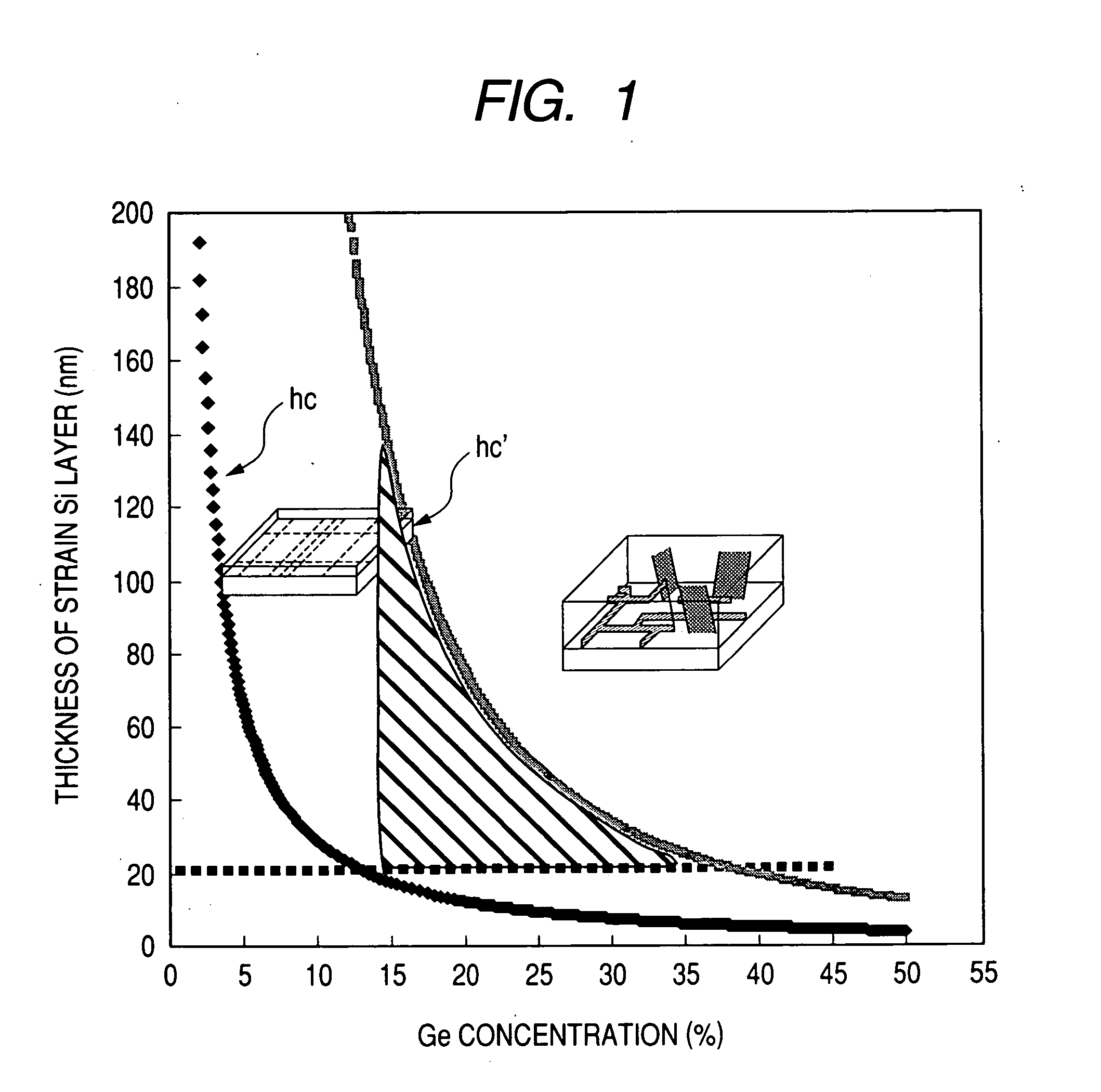
[0154] This example illustrates a field effect semiconductor device for high frequency power amplification in a case of setting a relation for the strained Si film thickness for channel and offset portions to the first case in the means of the present invention described previously. That is, this is a case in which the relation for each of film thickness is: 0.5 hch≦hoff

[0155]FIG. 6 is a cross sectional structural view showing a relation of the strained Si film thickness in Example 1.

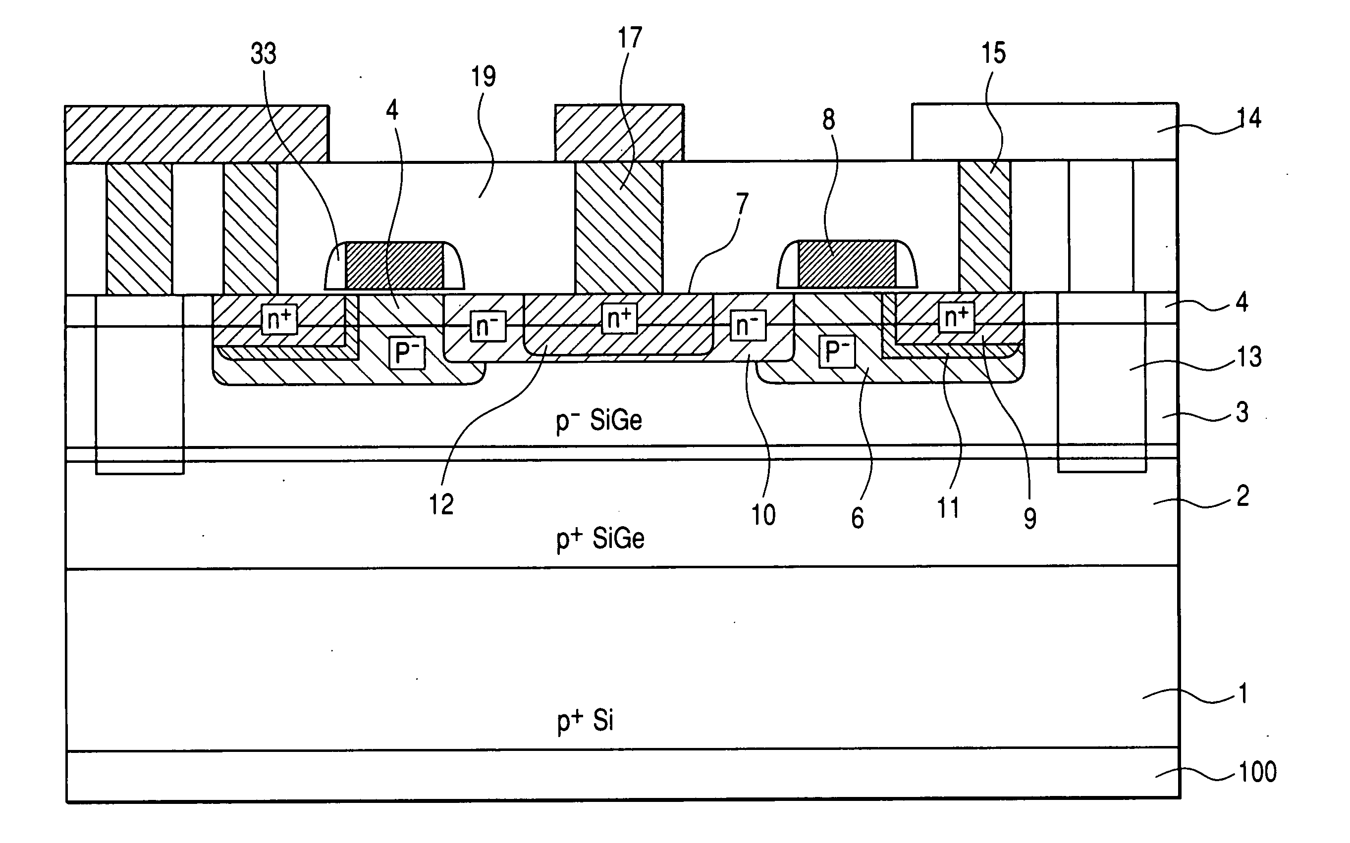
[0156] At first, a cross sectional structure of a field effect semiconductor device of Example 1 is to be described specifically with reference to FIG. 3 and FIG. 19.

[0157] Referring to FIG. 3, a basic stacked structure of this example is to be described. In the stacked semiconductor structure of this example, a P-type low resistance first SiGe layer 2, a P-type high resistance second SiGe layer 3, and a P-type high resistance strained Si layer 4 are stacked in this order above a P-ty...

example 2

[0175] This example illustrates a field effect semiconductor device for high frequency power amplification in a case of setting a relation of the strained Si film thickness for channel and offset portions to the first case and as: hch

[0176] The basic structure and manufacturing steps are similar to those shown in Example 1. This is different from Example 1 in that growing of thickness and fabrication are controlled such that the relation of strained Si film thickness for the channel and offset portions is: hch

[0177] The relation of film thickness as shown in FIG. 8 is attained by fabricating the gate electrode 8 and then epitaxially growing a second conduction type Si film at an impurity concentra...

example 3

[0178] This example illustrates a field effect semiconductor device for high frequency power amplification in a case of setting a relation of strained Si film thickness for channel and offset portions to the second case. That is, in the second case, relations of the film thickness are defined as: hch≦hc

[0179] The basic structure and manufacturing steps are similar to those shown in Example 1. This is different from Example 1 in that growing of thickness and fabrication are controlled such that the relation of strained Si film thickness for the channel and offset portions is: hch≦hc

[0180]FIG. 9 is an explanatory view showing the state. In this example, the strained Si film thickness for the offset portion is larger than the strained Si film thickness below the channel and while the former is less than the critical film thickness, the latter is more than the critical film thickness. Accordingly, appropriate countermeasures have to be applied in order not to increase the ...


PUM


Abstract

In a field effect semiconductor device for high frequency power amplification, it is difficult to achieve size reduction and increased efficiency simultaneously while ensuring voltage withstanding. A further improvement in efficiency is attained by using a strained Si channel for LDMOS at an output stage for high frequency power amplification. Further, the efficiency is improved as much as possible while decreasing a leak current, by optimizing the film thickness of the strained Si layer having a channel region, inactivation of defects and a field plate structure.

Description

CLAIM OF PRIORITY [0001] The present application claims priority from Japanese applications JP 2004-299718 filed on Oct. 14, 2004 and JP 2005-271758 filed on Sep. 20, 2005, the contents of which are hereby incorporated by reference into this application. BACKGROUND OF THE INVENTION [0002] 1. Field of the Invention [0003] The present invention relates to a field effect semiconductor device and, more in particular, it relates to a technique which is effective when applied to a field effect semiconductor device for high frequency power amplification with 800 MHz or higher used in mobile communication equipment. [0004] 2. Description of Related Art [0005] Along with rapid popularization of mobile communication terminals in recent years, a power amplifier for use in mobile terminals of lower power consumption and higher efficiency has been demanded more and more. The power amplification device in such application has employed a transistor using a compound semiconductor (HBT), an insulate...

Claims


Application Information

Patent Timeline
IPC IPC(8): H01L31/109
CPCH01L21/823412H01L21/823425H01L21/823807H01L21/823814H01L29/1054H01L29/41758H01L29/4238H01L29/66659H01L29/7835
Inventor KIMURA, YOSHINOBUSUGII, NOBUYUKIKIMURA, SHINICHIROTSUCHIYA, RYUTASAITO, SHINICHI
Owner RENESAS TECH CORP
Why Eureka
Try Eureka