Display device and fabrication method thereof

Inactive Publication Date: 2008-03-27
PANASONIC LIQUID CRYSTAL DISPLAY CO LTD +1
View PDF4 Cites 21 Cited by
  • Summary
  • Abstract
  • Description
  • Claims
  • Application Information

AI Technical Summary

Benefits of technology

[0016]By differentiating the film thickness of the amorphous semiconductor before crystallization in the SELAX-TFT area from that in the ELA-TFT area, it is possible to improve the characteristics of the SELAX-TFT and the throughput of the ELA crystallization. The improvement in characteristics of the SELAX-TFT allows implementation of higher-performance circuits on the substrate.
[0017]A plurality of semiconductor films, for example, silicon films, with different film thicknesses can be fabricated according to applications. For example, by fabricating a thin silicon film in the first layer to a thickness on the order of 30 to 50 nm and applying it to a thin film transistor in a pixel circuit, photoconductivity is reduced. Furthermore, by fabricating a thick silicon film in the second layer to a thickness on the order of 50 to 400 nm and applying it to a thin film transistor in a peripheral circuit including a drive circuit, low-voltage driving can be performed.
[0018]Increase in the film thickness of the

Problems solved by technology

Therefore, as the film thickness of silicon increases, it is necessary to reduce the beam width in order to increase the energy density

Method used


Image

  • Display device and fabrication method thereof
  • Display device and fabrication method thereof
  • Display device and fabrication method thereof

Examples


first embodiment

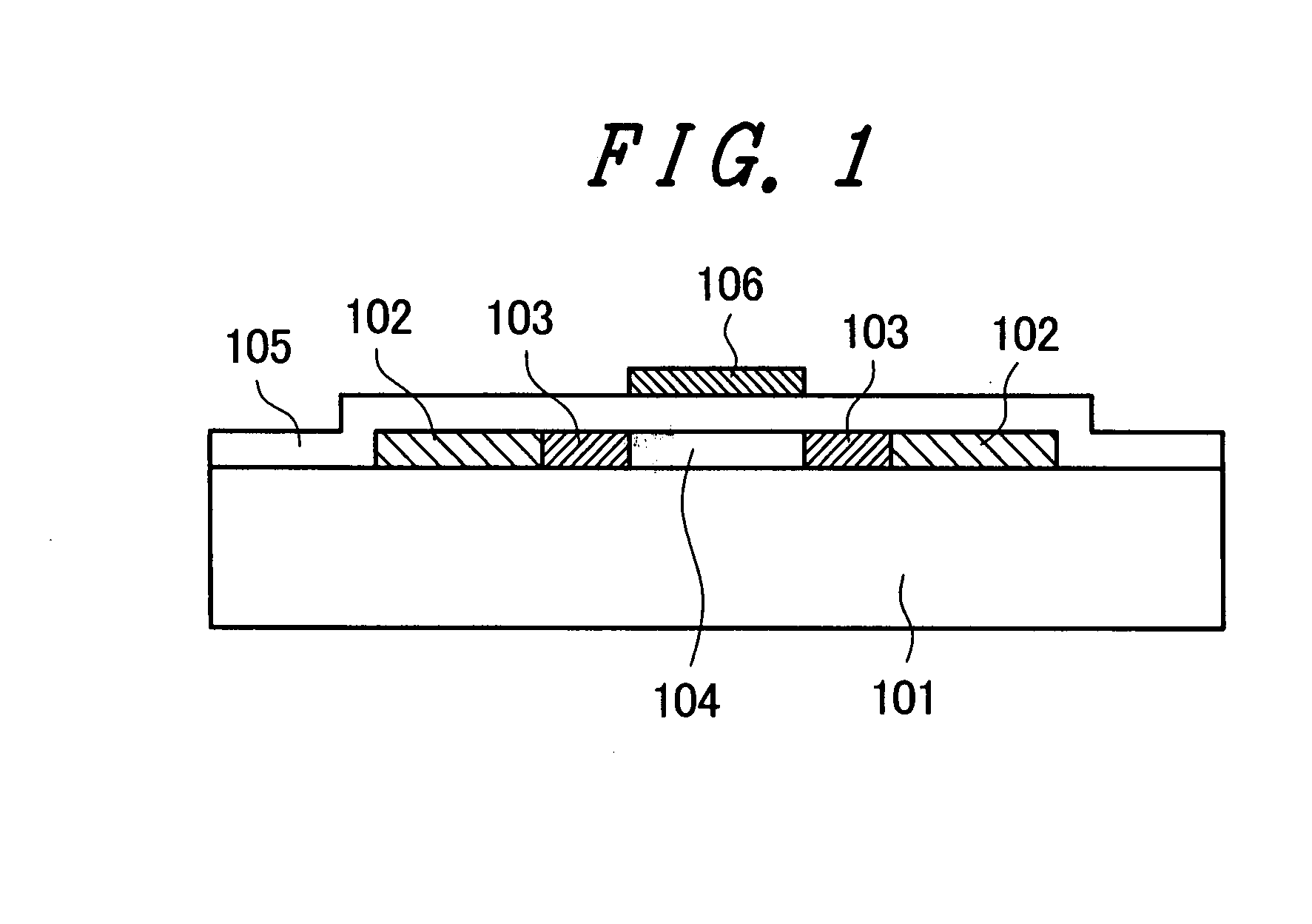
[0039]FIG. 1 is a cross-sectional view of a top-gate TFT for explaining a first embodiment of the invention. When the top-gate TFT is an n-channel TFT, a polysilicon layer 104 on a glass substrate 101 has source / drain areas 102 as well as LDD areas 103 for electric field reduction. When the top-gate TFT is a p-channel TFT, typically, no LDD area 103 is formed. On the resultant structure, a gate insulating film layer 105 and a gate metal layer 106 are formed.

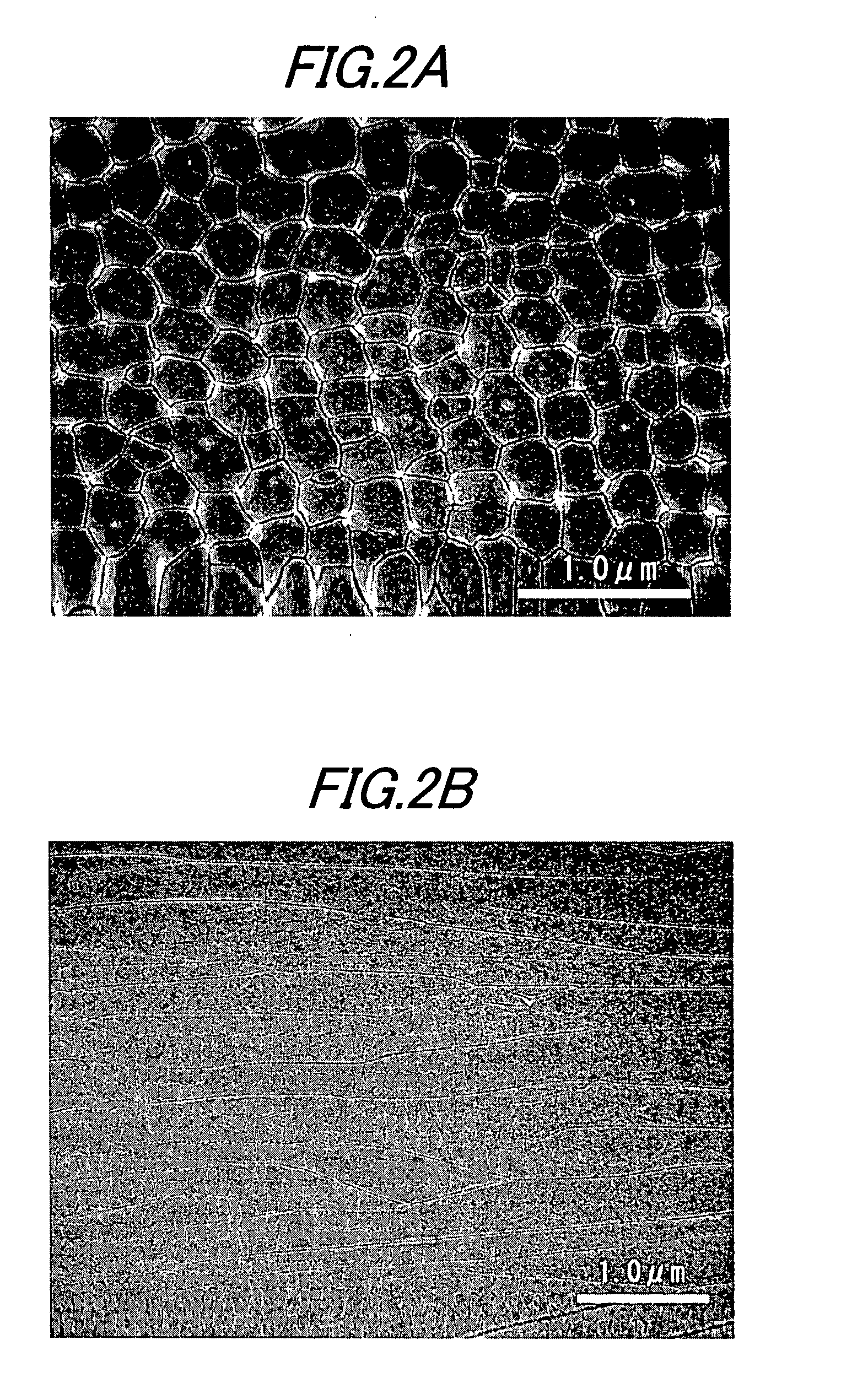
[0040]FIG. 2A shows a scanning electron micrograph of crystal grains crystallized in an ELA apparatus (hereinafter referred to as ELA crystal). ELA crystallization uses a pulse laser in its crystallization process, so that the length of the crystal growth time is reduced and hence particulate crystal grains are obtained, the diameter of which ranges from approximately 0.3 to 1 μm. On the other hand, FIG. 2B shows a scanning electron micrograph of crystal grains crystallized in a SELAX apparatus (hereinafter referred to as SELAX c...

second embodiment

[0061]FIGS. 12A to 12F explain a fabrication process flow that is similar to that shown in FIG. 7 and describes a second embodiment of the invention. In FIG. 12, channel implantation may be additionally performed to the SELAX-TFT portion. To control threshold voltages Vth for the ELA-TFT and the SELAX-TFT, the channel implantation concentration may be changed. After an amorphous silicon layer 109 is deposited over the substrate in a CVD apparatus, as in FIGS. 7A and 7B, an impurity, such as boron or phosphorus, is implanted into the amorphous silicon layer 109 (FIGS. 12A and 12B). This impurity allows adjustment of the threshold voltages Vth for the ELA-TFT and the SELAX-TFT.

[0062]Since increase in film thickness of the silicon layer enhances the carrier mobility in the thin film transistor, the TFT can be configured in such a way that the source and drain are disposed perpendicular to the crystal growth direction (vertical SELAX-TFT). The SELAX-TFT typically has satisfactory operat...

third embodiment

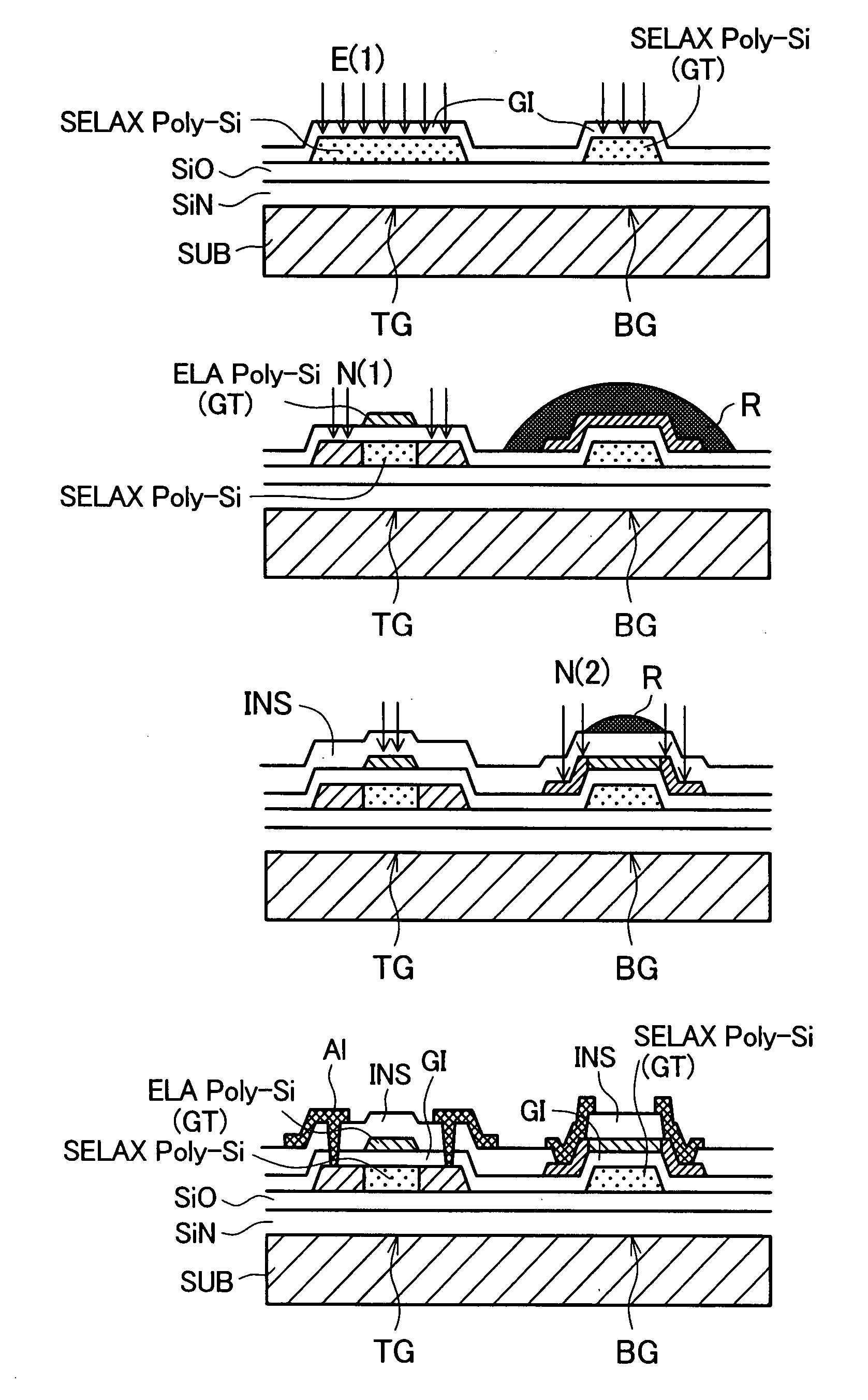
[0069]FIG. 13 is process flow diagrams for explaining a third embodiment of the invention. The third embodiment is implemented in the order from Process 1 (hereinafter labeled as P-1) to P-6 shown in FIG. 13. First, SiN and SiO are deposited in this order as underlying films on a glass substrate SUB. Amorphous silicon is deposited on these underlying films to a film thickness on the order of 30 to 70 nm, preferably 45 to 55 nm. Then, ELA crystallization is used to form ELA polysilicon (ELA poly-Si) followed by patterning. A gate insulating film GI(1) is then deposited to cover the ELA polysilicon (ELA poly-Si) and ion implantation E1 for threshold voltage adjustment is performed (P-1).

[0070]Amorphous silicon is deposited to a film thickness on the order of 50 to 400 nm, preferably 100 to 300 nm, and a continuous-wave laser beam is applied thereto to form pseudo single crystal silicon (SELAX poly-Si). A photolithography process including resist application, patterned exposure, and de...


PUM


Abstract

Improvement in characteristics of a SELAX-TFT and throughput of ELA crystallization is achieved. When a thin film transistor using pseudo single crystal semiconductor and a thin film transistor using particulate polysilicon semiconductor are formed on a single substrate, the film thickness of an amorphous semiconductor film before crystallization in the pseudo single crystal semiconductor portion is greater than that in the polysilicon semiconductor portion.

Description

[0001]The present application claims priority from Japanese applications JP2006-2262884 filed on Sep. 27, 2006, the content of which is hereby incorporated by reference into this application.BACKGROUND OF THE INVENTION[0002]The present invention relates to a method for fabricating a thin film transistor, a display device having a circuit using a thin film transistor fabricated by the fabrication method, and a method for fabricating the display device.[0003]As a display panel of a flat panel display device (FPD), a system-in-panel is in practical use in which not only a pixel section but a peripheral circuit including a drive circuit are built on a substrate that forms the display panel. To achieve such a system-in-panel, it is desirable to use a polycrystalline silicon (Si) layer (referred to as a polysilicon layer, a p—Si layer, an ELA silicon layer or the like) for a low-performance thin film transistor (TFT) circuit section, such as a pixel circuit section, which does not need re...

Claims


Application Information

Patent Timeline
IPC IPC(8): H01L27/15H01L21/00
CPCH01L21/02532H01L21/02675H01L21/268H01L29/04H01L29/0657H01L29/42384H01L27/1285H01L29/66765H01L29/78675H01L29/78678H01L27/1233H01L27/1237H01L27/1251H01L29/66757H01L27/1222H01L27/1229
Inventor MIYAKE, HIDEKAZUITOGA, TOSHIHIKOOUE, EIJINODA, TAKESHI
Owner PANASONIC LIQUID CRYSTAL DISPLAY CO LTD
Why Eureka
Try Eureka