Underlayer Coating Forming Composition for Lithography Containing Naphthalene Ring Having Halogen Atom

Active Publication Date: 2007-10-11
NISSAN CHEM IND LTD
View PDF12 Cites 24 Cited by
  • Summary
  • Abstract
  • Description
  • Claims
  • Application Information

AI Technical Summary

Benefits of technology

[0037] The underlayer coating forming composition for lithography of the present invention can provide an underlayer coating that can use as an anti-reflective coating effectively absorbing light reflected from a semiconductor substrate and causing no intermixing with a photoresist, in micro-processing by use of KrF excimer laser beam (wavelength 248 nm) and ArF excimer laser beam (wavelength 193 nm) and the like.
[0038] The underlayer coating forming composition of the present invention can provide an excellent underlayer coating that has a high dry etching rate compared with photoresists, and cause no intermixing with photoresists.
[0039] The underlayer coating forming composition for lithography of the present invention can attain a high filling property inside holes without occurrence of void (gap) in semiconductor

Problems solved by technology

Along with this change, influences of reflection from a substrate have become serious problems.
However, it is difficult to apply organic material for anti-reflective coating on a substrate h

Method used


Image

  • Underlayer Coating Forming Composition for Lithography Containing Naphthalene Ring Having Halogen Atom
  • Underlayer Coating Forming Composition for Lithography Containing Naphthalene Ring Having Halogen Atom
  • Underlayer Coating Forming Composition for Lithography Containing Naphthalene Ring Having Halogen Atom

Examples


synthetic example 1

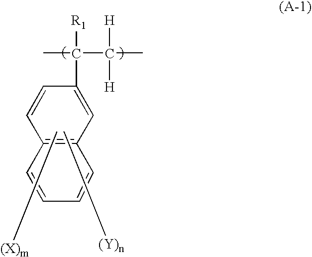
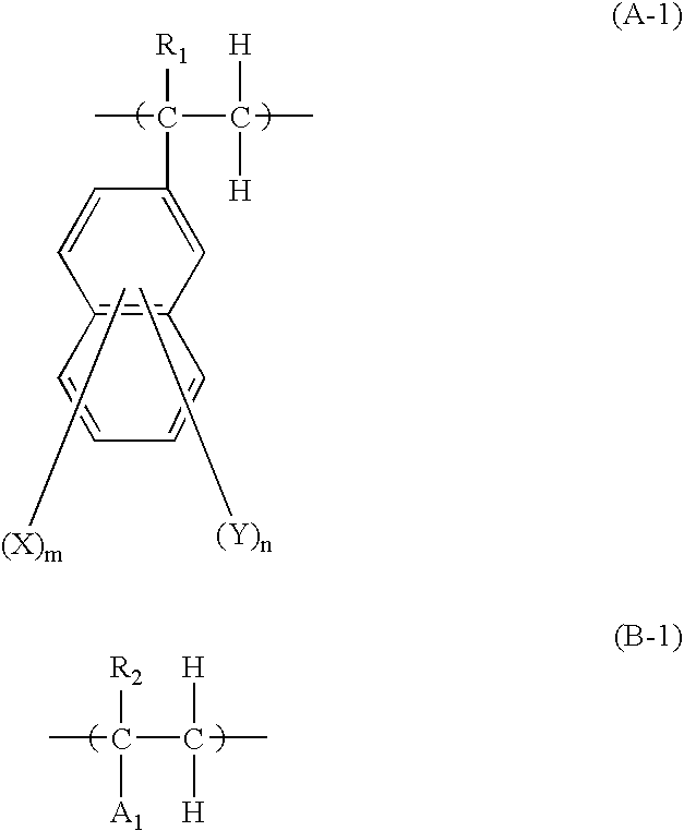
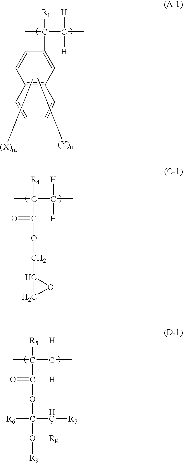
[0123] In 17.97 g of propylene glycol monomethyl ether acetate, 2.00 g of 1-ethoxyethyl methacrylate (product of Honshu Chemical Industry Co., Ltd.), 1.799 g of glycidyl methacrylate, and 5.902 g of 8-bromo-2-vinylnaphthalene (product of Nippon Steel Chemical Co., Ltd.) were dissolved, nitrogen was flowed to the reaction solution for 30 minutes, and then the temperature was raised to 70° C. While maintaining the reaction solution at 70° C., 0.077 g of azobisisobutyronitrile and 0.077 g of 1-dodecane thiol were added. After stirring under nitrogen atmosphere at 70° C. for 8 hours, 0.021 g of 4-methoxyphenol was added to obtain a solution containing a copolymer of 1-ethoxyethyl methacrylate, glycidyl methacrylate and 8-bromo-2-vinylnaphthalene. GPC analysis of the resulting polymer showed that it had a number average molecular weight Mn of 15000 and a weight average molecular weight Mw of 28500 (in terms of standard polystyrene).

synthetic example 2

[0124] In 25.7 g of propylene glycol monomethyl ether acetate, 2.0 g of 2-hydroxyethyl acrylate and 16.08 g of 8-bromo-2-vinylnaphthalene (product of Nippon Steel Chemical Co., Ltd.) were dissolved, nitrogen was flowed to the reaction solution for 30 minutes, and then the temperature was raised to 70° C. While maintaining the reaction solution at 70° C., 0.18 g of azobisisobutyronitrile and0.18 g of 1-dodecane thiol were added. After stirring under nitrogen atmosphere at 70° C. for 8 hours, 0.05 g of 4-methoxyphenol was added to obtain a solution containing a copolymer of hydroxyethyl acrylate and 8-bromo-2-vinylnaphthalene. GPC analysis of the resulting polymer showed that it had a number average molecular weight Mn of 10000 and a weight average molecular weight Mw of 24000 (in terms of standard polystyrene).

synthetic example 3

[0125] In 179.7 g of propylene glycol monomethyl ether acetate, 20.0 g of 1-ethoxyethyl methacrylate (product of Honshu Chemical Industry Co., Ltd.), 17.99 g of glycidyl methacrylate, and 39.04 g of 2-vinyinaphthalene (product of Nippon Steel Chemical Co., Ltd.) were dissolved, nitrogen was flowed to the reaction solution for 30 minutes, and then the temperature was raised to 70° C. While maintaining the reaction solution at 70° C., 0.77 g of azobisisobutyronitrile and 0.77 g of 1-dodecane thiol were added. After stirring under nitrogen atmosphere at 70° C. for 8 hours, 0.21 g of 4-methoxyphenol was added to obtain a solution containing a copolymer of 1-ethoxyethyl methacrylate, glycidyl methacrylate and 2-vinylnaphthalene. GPC analysis of the resulting polymer showed that it had a number average molecular weight Mn of 10500 and a weight average molecular weight Mw of 21000 (in terms of standard polystyrene).


PUM

PropertyMeasurementUnit
Compositionaaaaaaaaaa

Abstract

There is provided an underlayer coating forming composition for lithography, and an underlayer coating having a high dry etching rate compared with photoresist, and causing no intermixing with the photoresist, which are used in lithography process of manufacture of semiconductor device. Concretely, it is an underlayer coating forming composition comprising a polymer having a structural unit containing naphthalene ring substituted with halogen atom in a molar ratio of 0.3 or more in the structural units constituting the polymer, a solvent.

Description

TECHNICAL FIELD [0001] The present invention relates to a novel underlayer coating forming composition for lithography, an underlayer coating formed from the composition and a method for forming photoresist pattern by use of the underlayer coating. In addition, the present invention relates to an underlayer coating that can be used for an underlayer anti-reflective coating formed between a semiconductor substrate and a photoresist for preventing reflection of exposure irradiation light from the semiconductor substrate in a lithography process of the manufacture of semiconductor devices, a flattening coating for flattening a semiconductor substrate having unevenness, a coating for preventing contamination of a photoresist layer due to substances generated from a semiconductor substrate on baking under heating, and the like; an underlayer coating forming composition for lithography for forming the underlayer coating. Further, the present invention relates to a composition for forming ...

Claims


Application Information

Patent Timeline
IPC IPC(8): C08F12/14H01L21/027
CPCC08F220/28C08F220/32G03F7/11G03F7/094G03F7/091C08F220/281C08F220/325C08F12/14C08F216/06C08F216/14
Inventor TAKEI, SATOSHISAKAGUCHI, TAKAHIROENOMOTO, TOMOYUKI
Owner NISSAN CHEM IND LTD
Why Eureka
Try Eureka