

Light-emitting device
a technology of light-emitting devices and light-emitting devices, which is applied in the direction of discharge tube luminescnet screens, energy-saving lighting, sustainable buildings, etc., can solve the problems of inability to employ such a light-emitting device as an illumination source, thiogallate and sulfide are chemically unstable, and sulfide tends to decompose, etc., to achieve high color rendering properties, high efficiency, and high efficiency
- Summary
- Abstract
- Description
- Claims
- Application Information
AI Technical Summary
Benefits of technology
Problems solved by technology
Method used
Image

Examples
example 1
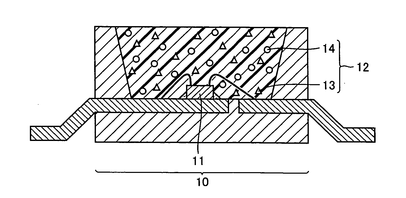
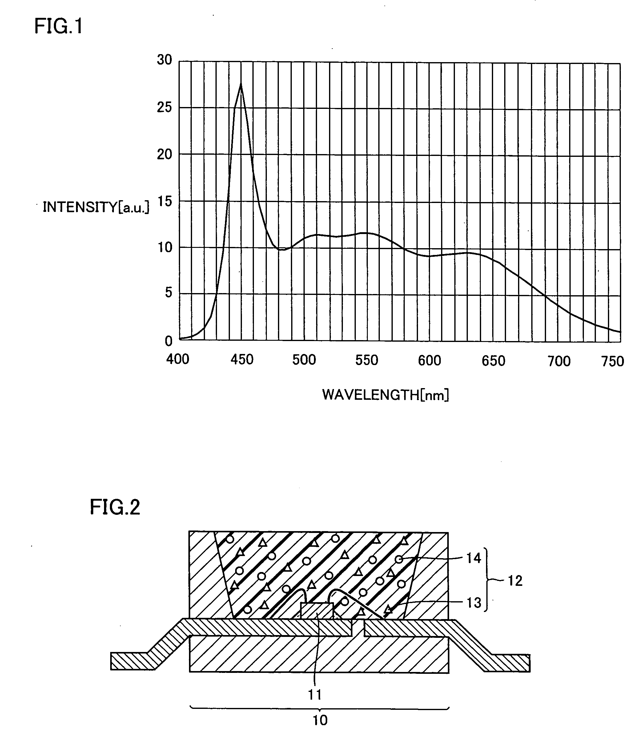
[0090]FIG. 2 is a schematic longitudinal cross-sectional view of a light-emitting device of Example 1 of the present invention. A light-emitting device 10 includes a light-emitting element 11 emitting primary light, and a wavelength conversion portion 12 absorbing at least a part of the primary light and emitting secondary light having a wavelength equal to or longer than wavelength of the primary light. Wavelength conversion portion 12 contains a red light-emitting phosphor 13 and a green light-emitting phosphor 14 diffused in a resin.
[0091] In Example 1, a gallium nitride (GaN)-based semiconductor having a peak wavelength at 450 nm was used as the light-emitting element. Ca3(Sc0.85Ce0.15)2(SiO4)3 (particle size: 8.9 μm) and (Ca0.98Eu0.02)AlSiN3 (particle size: 3.8 μm) were used as the green light-emitting phosphor and the red light-emitting phosphor respectively, to fabricate the wavelength conversion portion. Mixture of the green light-emitting phosphor and the red light-emittin...
example 2
[0093] A gallium nitride (GaN)-based semiconductor having a peak wavelength at 435 nm was used as the light-emitting element. Fifty weight % 2(Ba0.60Sr0.38Eu0.02)O.SiO2 having a particle size of 9.3 μm and 50 weight % 2(Sr0.80Ba0.18Eu0.02)O.SiO2 having a particle size of 10.5 μm, and (Ca0.94Mg0.05Eu0.01)(Al0.99In0.01)SiN3 having a particle size of 3.61 μm were used as the green light-emitting phosphor and the red light-emitting phosphor respectively, to fabricate the wavelength conversion portion. Mixture of combination of the green light-emitting phosphors and the red light-emitting phosphor at a weight ratio of 1:0.31 was diffused in a silicone resin, followed by forming, thereby fabricating the wavelength conversion portion. The light-emitting device in Example 2 structured as shown in FIG. 2 was thus fabricated.
example 3
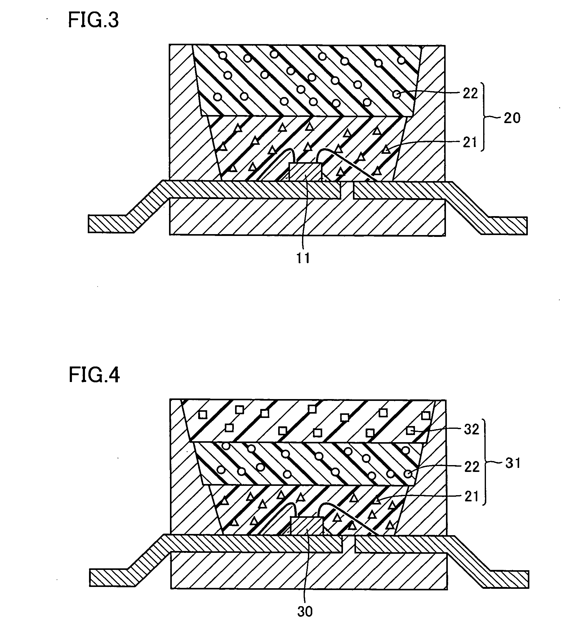
[0095]FIG. 3 is a schematic longitudinal cross-sectional view of the light-emitting device of Example 3 of the present invention. The light-emitting device includes light-emitting element 11 emitting primary light and a wavelength conversion portion 20 absorbing at least a part of the primary light and emitting secondary light having a wavelength equal to or longer than wavelength of the primary light. Wavelength conversion portion 20 includes a resin layer containing diffused red light-emitting phosphor (red light-emitting phosphor layer) 21 and a resin layer containing diffused green light-emitting phosphor (green light-emitting phosphor layer) 22. Red light-emitting phosphor layer 21 is arranged proximate to light-emitting element 11, and green light-emitting phosphor layer 22 is layered thereon.
[0096] In Example 3, a gallium nitride (GaN)-based semiconductor having a peak wavelength at 435 nm was used as the light-emitting element. (Ca0.8Mg0.2)3(Sc0.75Ga0.15Ce0.10)2(SiO4)3 havi...
PUM
 Abstract
Description
Claims
Application Information