Semiconductor device and method of manufacturing the same, circuit board and electronic instrument

a semiconductor and semiconductor chip technology, applied in the direction of semiconductor/solid-state device details, semiconductor devices, electrical apparatus, etc., can solve the problems of processing complexity or additional materials cost, and the size of semiconductor chips is limited

Inactive Publication Date: 2001-01-30
SEIKO EPSON CORP
View PDF7 Cites 74 Cited by
  • Summary
  • Abstract
  • Description
  • Claims
  • Application Information

AI Technical Summary

Problems solved by technology

However, for the actual connection of the semiconductor device, the are problems of the process becoming complicated or additional materials cost being incurred, because for example the mounting is on a substrate re

Method used


Image

  • Semiconductor device and method of manufacturing the same, circuit board and electronic instrument
  • Semiconductor device and method of manufacturing the same, circuit board and electronic instrument
  • Semiconductor device and method of manufacturing the same, circuit board and electronic instrument

Examples


first embodiment

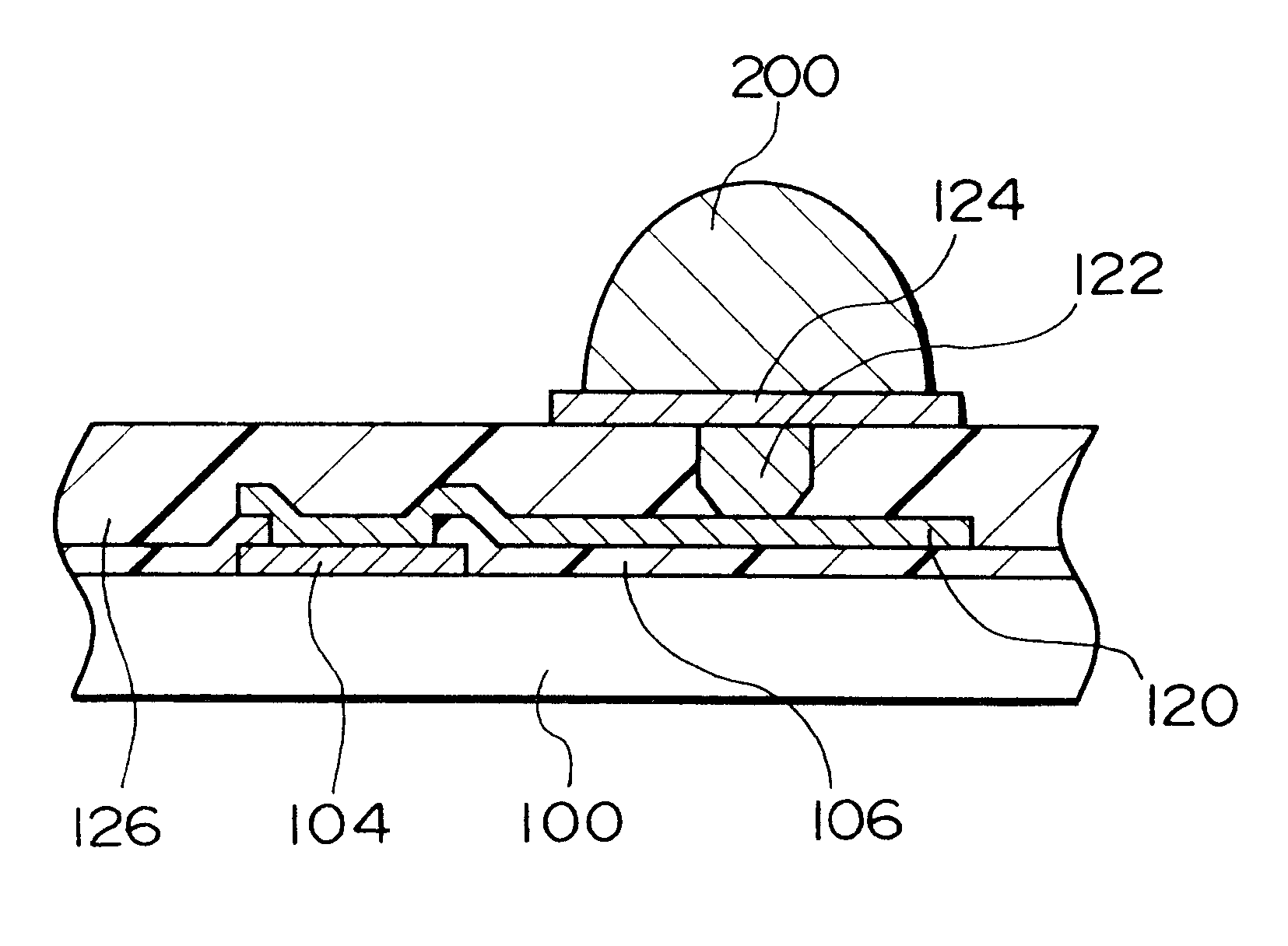
FIG. 1 shows the semiconductor device of the present invention. The semiconductor device shown in FIG. 1 comprises a semiconductor chip (semiconductor chip) 100 on which is provided a bump 200 with a stress relief function interposed. This configuration allows flip-chip having a stress relief function, and can also be classified as CSP (Chip Size / Scale Package).

The semiconductor chip 100 comprises a plurality of elements such as gates (not shown in the drawings). On the semiconductor chip 100, a plurality of electrodes 104 are formed. On the surface of the semiconductor chip 100 on which the electrodes 104 are formed, an insulating layer 106 is formed, avoiding the area where the electrodes 104 are provided. The insulating layer 106 may be formed as a silicon oxide film. It should be noted that, as other examples, a silicon nitride film, or polyimide, or the like may be used. To the electrodes 104 are connected an interconnect layer 120 is connected, and the interconnect layer 120 e...

second embodiment

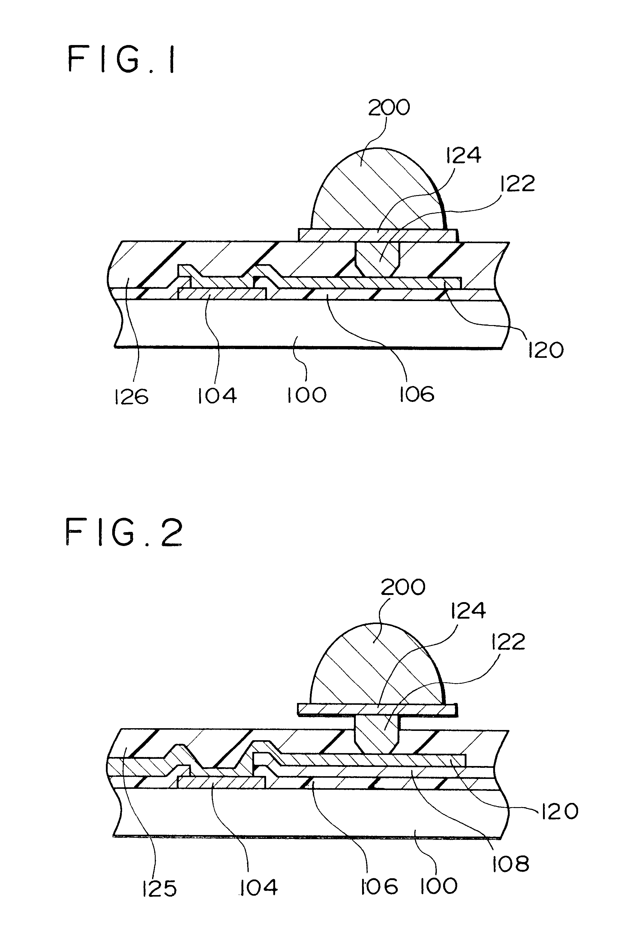
FIGS. 4A to 6B show the method of manufacturing a second embodiment of the semiconductor device of the present invention. In this embodiment, as shown in FIG. 4A, a semiconductor chip 100 is provided with electrodes 104 and an interconnect layer 120 connected to the electrodes 104. It should be noted that on the semiconductor chip 100 an insulating layer 106 is formed, and an interconnect layer 120 is formed on the insulating layer 106.

Then, a conducting layer is provided on the interconnect layer 120, at a position avoiding where the electrodes 104 are provided, and an underlying metal layer is provided on the conducting layer. In more detail, the following first to sixth steps are carried out.

First Step

As shown in FIG. 4A, at least on the interconnect 120, and at least in a region including the forming region of the conducting layer, a first conducting material 130 is formed. The first conducting material 130 may be formed over the whole surface of the semiconductor chip 100 on wh...

third embodiment

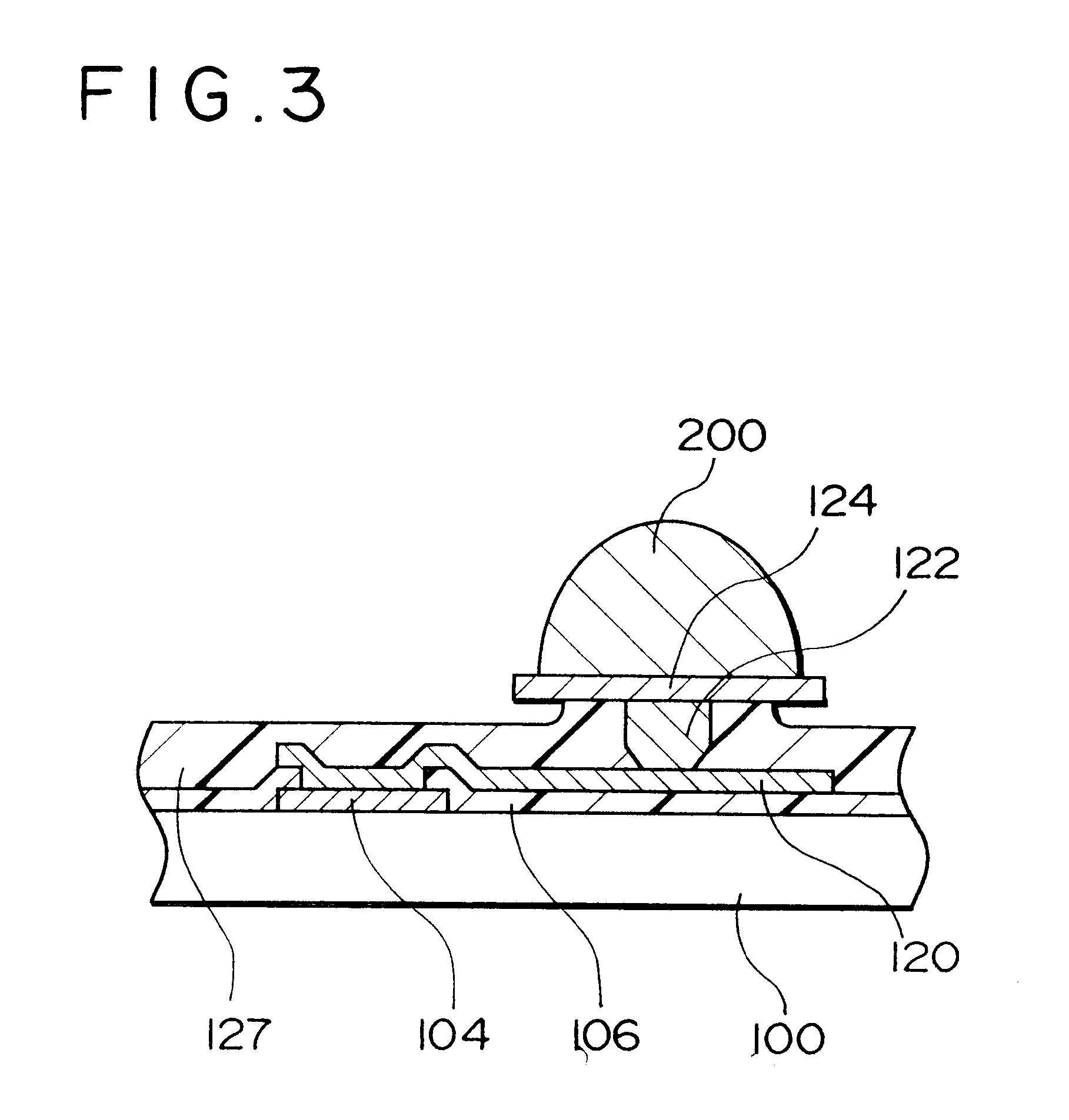
FIGS. 8 to 8C show the method of manufacturing a third embodiment of semiconductor device of the present invention.

Steps of Providing a Conducting Layer and the Resin Layer

First Step

As shown in FIG. 7A, a resin layer 160 is formed to have an opening 162 which is provided on the interconnect 120 at a region where the conducting layer is formed.

Second Step

As shown in FIGS. 7A and 7B, the opening portion of a stencil is aligned with the opening 162, and by means of a squeegee 166 the opening 162 is filled with a conductive paste 168. In other words, screen printing is carried out. Here, the conductive paste 168 has a conductive filler distributed in a binder. By means of screen printing, a plurality of openings 162 can be filled with the conductive paste 168 in a single operation. Alternatively, dispensing printing may equally be used. Dispensing printing is appropriate when the opening 162 is deep.

Third Step

As shown in FIG. 7C, the conductive paste 168 is heated, and the binder is har...


PUM


Abstract

A semiconductor device and method of manufacturing the same, a circuit board and an electronic instrument are such that without substrate material selection or additional steps after connection, connection reliability can be assured, while direct connection to a substrate is possible, further allowing an electronic instrument to be made more compact and lightweight. The semiconductor device comprises a semiconductor chip (100) having electrodes (104), an interconnect layer (120) connected to the electrodes (104), a conducting layer (122) provided on the interconnect layer (120) avoiding the area of the electrodes (104), an underlying metal layer (124) having a size larger than the peripheral outline of the conducting layer (122) provided on the conducting layer (122) and easier to be deformed than the conducting layer (122), bumps (200) provided on the underlying metal layer (124), and a resin layer (126) provided on the periphery of the conducting layer (122).

Description

The present invention relates to a semiconductor device and method of manufacturing the same, a circuit board and an electronic instrument.BACKGROUND OF ARTConventionally, the underlying metal of solder bumps is formed by a barrier metal thin film directly formed on the electrode (normally aluminum) and formed at substantially the same size, and a metal thin film formed directly on the barrier metal thin film at substantially the same size and with good wettability with solder. The same construction is used, even when an interconnect layer is formed on a semiconductor chip.In recent years, with the more compact design of electronic instruments, there has been an active move toward directly connecting a semiconductor device having solder bumps to the substrate, to provide even more compact and lightweight electronic instruments. In view of this, there is an increasing demand for a reliable connection of the semiconductor chip to a substrate with a greatly differing coefficient of the...

Claims


Application Information

Patent Timeline
IPC IPC(8): H01L23/48H01L23/485
CPCH01L24/13H01L24/11H01L2224/1147H01L2924/0002H01L2924/01013H01L2924/01027H01L2924/01029H01L2924/0103H01L2924/01033H01L2924/01061H01L2924/01078H01L2924/01079H01L2924/01082H01L2924/19041H01L2924/19043H01L2924/01024H01L2924/01047H01L2924/014H01L2224/11902H01L2224/0383H01L2224/03436H01L2224/036H01L2224/05557H01L2224/05568H01L2224/13099H01L2224/0401H01L2924/00012H01L2924/00014H01L2924/00H01L2224/05552H01L2924/351H01L2924/12042H01L2224/11H01L2224/13H01L2224/051H01L2224/05111H01L2224/05139H01L2224/05144H01L2224/05147H01L2224/05155H01L2224/05171H01L2224/05647H01L2224/13007H01L24/03H01L24/05H01L2224/023H01L2924/0001H01L23/12
Inventor NOZAWA, KAZUHIKO
Owner SEIKO EPSON CORP
Why Eureka
Try Eureka